Friday, December 12, 2014
Plus and Minus DC Power Supply

This is a classic example of a regulated DC power supply that produces both a positive 15v and a negative 15v from a 20vac wall adapter.
Solar Battery Charger Circuit Schematic

Here is a solar charger circuit that is used to charge Lead Acid or Ni-Cd batteries using the solar energy power. The circuit harvests solar energy to charge a 6 volt 4.5 Ah rechargeable battery for various applications. The charger has Voltage and Current regulation and Over voltage cut off facilities.
Power Amplifier
300w Sub-woofer Power Amplifier - High power amps are not too common as projects, since they are by their nature normally difficult to build and are expensive.
LM3886 Power Amplifier - The LM3886 is a high-performance audio power amplifier capable of delivering 68W of continuous average power to a 4 ohm load and 38W into 8 ohm load.
2.3 GHz Power Amplifier - 2 schematic which contains prototype and real one.
20 Watt Class-A Power Amplifier - This amp uses the basic circuitry of the 60W power amp but has been modified for true Class-A operation.
20 Watt / Channel Stereo Power Amplifier - This project is based almost directly on the typical application circuit in the National Semiconductor specification sheet.
Simple Audio Power Amp - This simple audio power amplifier was originally designed for a circuit board workshop conducted by the OSU IEEE Student Group.
Death of Zen (DoZ) - A New Class-A Power Amp - This project design specifically for headphones.
Simple Current Feedback Power Amplifier - The first version of the amp uses a single power supply and capacitor coupled speaker.
Single Chip 50 Watt / 8 Ohm Power Amplifier - This project is based almost directly on the typical application circuit in the National Semiconductor specification sheet.
Soft-Start Circuit For Power Amps - The circuit presented in the website is designed to limit inrush current to a safe value.
170W Audio Power Amplifier - Suitable for self-powered speakers, sub-woofers and quality car boosters.
Read More..
LM3886 Power Amplifier - The LM3886 is a high-performance audio power amplifier capable of delivering 68W of continuous average power to a 4 ohm load and 38W into 8 ohm load.
2.3 GHz Power Amplifier - 2 schematic which contains prototype and real one.
20 Watt Class-A Power Amplifier - This amp uses the basic circuitry of the 60W power amp but has been modified for true Class-A operation.
20 Watt / Channel Stereo Power Amplifier - This project is based almost directly on the typical application circuit in the National Semiconductor specification sheet.
Simple Audio Power Amp - This simple audio power amplifier was originally designed for a circuit board workshop conducted by the OSU IEEE Student Group.
Death of Zen (DoZ) - A New Class-A Power Amp - This project design specifically for headphones.
Simple Current Feedback Power Amplifier - The first version of the amp uses a single power supply and capacitor coupled speaker.
Single Chip 50 Watt / 8 Ohm Power Amplifier - This project is based almost directly on the typical application circuit in the National Semiconductor specification sheet.
Soft-Start Circuit For Power Amps - The circuit presented in the website is designed to limit inrush current to a safe value.
170W Audio Power Amplifier - Suitable for self-powered speakers, sub-woofers and quality car boosters.
Mini Subwoofer Circuit 22W

The subwoofer is a subwoofer or a speaker to reproduce low frequencies, devotee of 20 Hz to 150 Hz electronic circuit diagram below shows the details of a scheme of the main amplifier TDA1516 22 watt in 4 ohm car subwoofer driver. This device is designed for an existing stereo amplifier, often requires adding another blow to the music of driving a subwoofer.
Thursday, December 11, 2014
VHF Antenna Amplifier

A very simple antenna amplifier electronic circuit project can be designed using this circuit diagram.This antenna amplifier electronic circuit can be used for a frequency range between 1 and 300MHz.
This circuit antenna amplifier can be used for high frequency and VHF band ( for radio and TV) and will provide a 22 dB gain .This antenna amplifier electronic project has a very low noise , under 1.6dB .This VHF, FM amplifier circuit is constructed based on the BFT66 transistor connected in common emitter connection.
Thursday, November 20, 2014
A 4 Digit Keypad Controller Switch Circuit
This is a universal version of the Four-Digit Alarm Keypad . I have modified the design to free up the relay contacts. This allows the circuit to operate as a general-purpose switch. It also means that it can be used to control all of my Alarm Circuits. Ive used a SPCO/SPDT relay - but you can use a multi-pole relay if you wish.
The relay is energized by pressing a single key. Choose the key you want to use - and connect it to terminal "E". Choose the four keys you want to use to de-energize the relay - and connect them to "A B C & D". Wire the common to R1 and all the remaining keys to "F".
The Circuit is easy to use. When you press "E" - current through D2 & R9 turns Q6 on - and energizes the relay. The two transistors - Q5 & Q6 - form a "Complementary Latch". So - when you release the key - the relay will remain energized.
To de-energize the relay - you need to press keys "A B C & D" in the right order. When you do so - pin 10 of the IC goes high - and it turns Q4 on through R8. Q4 connects the base of Q6 to ground. This unlatches the complementary pair - and the relay drops out.
Any keys not wired to "A B C D & E" are connected to the base of Q3 by R7. Whenever one of these "Wrong" keys is pressed - Q3 takes pin 1 low and the code entry sequence fails. If "C" or "D" is pressed out of sequence - Q1 or Q2 will also take pin 1 low - with the same result. If you make a mistake while entering the code - simply start again.
The Keypad must be the kind with a common terminal and a separate connection for each key. On a 12-key pad, look for 13 terminals. The matrix type with 7 or 8 terminals will NOT do. With a 12-key pad - over 10 000 different codes are available. If you need a more secure code - use a bigger keypad with more "Wrong" keys wired to "F". A 16-key pad gives over 40 000 different codes.
Interface Relay with PNP transistor
One technique relay drivers from the microcontroller or computer can be made with the driver PNP transistors like the article "Interface Relays With PNP Transistor" ini.This circuit interface is simple and easily applied to a microcontroller or computer parallel port. Interface Relays With PNP Transistor uses 2 transistors 2N3904 and 2n2905/2N2907 UAH as a power relay drivers. The advantages of this circuit can menggeran relay with considerable power with TTL logic input from the computer and microcontroller. Source voltage required to follow the relay circuit is used, for example using a 12V relay, the source voltage to 12V or 24V relays the 24V voltage source. Detailed relay interface circuit and microcontroller or computer can be seen in the following figure.

Function diodes mounted parallel with the relay to prevent backflow into the transistor due to magnetic induction of the relay coil, therefore these diodes must be installed. For installation with a microcontroller or computer which need to be noticed is the Grund computer or microcontroller circuit must be connected to ground in series Interface Relays With this PNP transistors.
RS232 to RS485 Circuit
The new archetypal of RS485 advocate overcomes the RTS controlled botheration accomplished by our chargeless design. However, to do that requires a microprocessor, so there is a greater complication to the design. We advertise this unit, although currently we are attached our sales to barter who can pay by coffer alteration – which in absoluteness is bounded Australian companies.
This architecture has been almost agitation free, and if you crave quantities we can acclimate the adapter pinout to clothing your appliance – about again the accessory will no best fit the simple little D25 case in which you see it pictured.
 |
| RS232 to RS485 Circuit |
* Data (vs RTS) controlled – does not rely on PC handshake timing
* DB25 RS232 connector compatible with PC
* TxD and RxD translated from RS232 to RS485
* Direction of transmission controlled by Data
* Handshake loop the PC connection so it works with all software
* RS485 signals output on D9 male with lots of Ground pins
* Indicator LED(s) to show communications traffic
* Line powered – powered by RS232 handshake lines
* RS485 Termination resistor not included
* Pullup/Pulldown resistors on RS485 to establish line-idle condition
* Baud rate is dipswitch selectable 1200 – 115.2k
Wednesday, November 19, 2014
NIMH battery charger
Series NIMH Battery Charger with IC LT4060 is a NIMH battery charger is powerful, effective and efficient. Featur owned by IC LT4060 is a specialization of a NIMH battery charger. NIMH Battery Charger with IC LT4060 can perform safely charging NIMH batteries because it comes with a battery temperature protection is in charge and the peak level detection system of the battery voltage is in charge. Battery temperature protection system from the excessive use of NTC temperature sensor. Series NIMH Battery Charger with IC LT4060 also features a charging indicator that will light up when charging and will die when the battery is full. IC 4060 used in this NIMH battery charger from Linear Technology is a production that is designed special for NIMH battery charger.
Image Series NIMH Battery Charger with IC LT4060

Description Series NIMH Battery Charger with IC LT4060
R2 potentiometer used for setting the maximum temperature (at set at the value of 4K)
LED D1 is a battery charging indicator
Charger Power Transistor (Q1) can be replaced with PNP transistors are capable of a current of 3A - 5A
Simple Power Supply with 2 transistors
Power Supply in this post is using a regulator which is composed of 2 pieces of NPN transistor. A transistor acts as a power regulator and a transistor again serves as a controller output voltage. Power Supply has an adjustable output with a range of 6-12 VDC. The part that serves as a power regulator is Q1 TIP31. Then the controller output voltage is a voltage divider composed of R3, R4, VR1 and R2 provide bias to the base of Q2 to control the power regulator Q1. In a series of power supply is mounted 5.1 V zener diode which serves to make the minimum limit the output voltage with Q2.
Power Supply With transistor circuit is quite simple and can be made with the PCB holes, so for those who want to try to directly mempraktikannya. May the power supply circuit can be useful for readers, especially for friends who need a power supply circuit with the regulator transistor.
8051 Tutorial Part 1 Serial Communication
One of the 8051s many powerful features is its integrated UART, otherwise known as a serial port. The fact that the 8051 has an integrated serial port means that you may very easily read and write values to the serial port. If it were not for the integrated serial port, writing a byte to a serial line would be a rather tedious process requring turning on and off one of the I/O lines in rapid succession to properly "clock out" each individual bit, including start bits, stop bits, and parity bits.
However, we do not have to do this. Instead, we simply need to configure the serial ports operation mode and baud rate. Once configured, all we have to do is write to an SFR to write a value to the serial port or read the same SFR to read a value from the serial port. The 8051 will automatically let us know when it has finished sending the character we wrote and will also let us know whenever it has received a byte so that we can process it. We do not have to worry about transmission at the bit level--which saves us quite a bit of coding and processing time.
Setting the Serial Port Mode
The first thing we must do when using the 8051s integrated serial port is, obviously, configure it. This lets us tell the 8051 how many data bits we want, the baud rate we will be using, and how the baud rate will be determined.
First, lets present the "Serial Control" (SCON) SFR and define what each bit of the SFR represents:
| Bit | Name | Bit Addres | Explanation of Function |
| 7 | SM0 | 9Fh | Serial port mode bit 0 |
| 6 | SM1 | 9Eh | Serial port mode bit 1. |
| 5 | SM2 | 9Dh | Mutliprocessor Communications Enable (explained later) |
| 4 | REN | 9Ch | Receiver Enable. This bit must be set in order to receive characters. |
| 3 | TB8 | 9Bh | Transmit bit 8. The 9th bit to transmit in mode 2 and 3. |
| 2 | RB8 | 9Ah | Receive bit 8. The 9th bit received in mode 2 and 3. |
| 1 | TI | 99h | Transmit Flag. Set when a byte has been completely transmitted. |
| 0 | RI | 98h | Receive Flag. Set when a byte has been completely received. |
Additionally, it is necessary to define the function of SM0 and SM1 by an additional table:
| SM0 | SM1 | Serial Mode | Explanation | Baud Rate |
| 0 | 0 | 0 | 8-bit Shift Register | Oscillator / 12 |
| 0 | 1 | 1 | 8-bit UART | Set by Timer 1 (*) |
| 1 | 0 | 2 | 9-bit UART | Oscillator / 64 (*) |
| 1 | 1 | 3 | 9-bit UART | Set by Timer 1 (*) |
(*) Note: The baud rate indicated in this table is doubled if PCON.7 (SMOD) is set.
The SCON SFR allows us to configure the Serial Port. Thus, well go through each bit and review its function.
The first four bits (bits 4 through 7) are configuration bits.
Bits SM0 and SM1 let us set the serial mode to a value between 0 and 3, inclusive. The four modes are defined in the chart immediately above. As you can see, selecting the Serial Mode selects the mode of operation (8-bit/9-bit, UART or Shift Register) and also determines how the baud rate will be calculated. In modes 0 and 2 the baud rate is fixed based on the oscillators frequency. In modes 1 and 3 the baud rate is variable based on how often Timer 1 overflows. Well talk more about the various Serial Modes in a moment.
The next bit, SM2, is a flag for "Multiprocessor communication." Generally, whenever a byte has been received the 8051 will set the "RI" (Receive Interrupt) flag. This lets the program know that a byte has been received and that it needs to be processed. However, when SM2 is set the "RI" flag will only be triggered if the 9th bit received was a "1". That is to say, if SM2 is set and a byte is received whose 9th bit is clear, the RI flag will never be set. This can be useful in certain advanced serial applications. For now it is safe to say that you will almost always want to clear this bit so that the flag is set upon reception of any character.
The next bit, REN, is "Receiver Enable." This bit is very straightforward: If you want to receive data via the serial port, set this bit. You will almost always want to set this bit.
The last four bits (bits 0 through 3) are operational bits. They are used when actually sending and receiving data--they are not used to configure the serial port.
The TB8 bit is used in modes 2 and 3. In modes 2 and 3, a total of nine data bits are transmitted. The first 8 data bits are the 8 bits of the main value, and the ninth bit is taken from TB8. If TB8 is set and a value is written to the serial port, the datas bits will be written to the serial line followed by a "set" ninth bit. If TB8 is clear the ninth bit will be "clear."
The RB8 also operates in modes 2 and 3 and functions essentially the same way as TB8, but on the reception side. When a byte is received in modes 2 or 3, a total of nine bits are received. In this case, the first eight bits received are the data of the serial byte received and the value of the ninth bit received will be placed in RB8.
TI means "Transmit Interrupt." When a program writes a value to the serial port, a certain amount of time will pass before the individual bits of the byte are "clocked out" the serial port. If the program were to write another byte to the serial port before the first byte was completely output, the data being sent would be garbled. Thus, the 8051 lets the program know that it has "clocked out" the last byte by setting the TI bit. When the TI bit is set, the program may assume that the serial port is "free" and ready to send the next byte.
Finally, the RI bit means "Receive Interrupt." It funcions similarly to the "TI" bit, but it indicates that a byte has been received. That is to say, whenever the 8051 has received a complete byte it will trigger the RI bit to let the program know that it needs to read the value quickly, before another byte is read.
Setting the Serial Port Baud Rate
Once the Serial Port Mode has been configured, as explained above, the program must configure the serial ports baud rate. This only applies to Serial Port modes 1 and 3. The Baud Rate is determined based on the oscillators frequency when in mode 0 and 2. In mode 0, the baud rate is always the oscillator frequency divided by 12. This means if youre crystal is 11.059Mhz, mode 0 baud rate will always be 921,583 baud. In mode 2 the baud rate is always the oscillator frequency divided by 64, so a 11.059Mhz crystal speed will yield a baud rate of 172,797.
In modes 1 and 3, the baud rate is determined by how frequently timer 1 overflows. The more frequently timer 1 overflows, the higher the baud rate. There are many ways one can cause timer 1 to overflow at a rate that determines a baud rate, but the most common method is to put timer 1 in 8-bit auto-reload mode (timer mode 2) and set a reload value (TH1) that causes Timer 1 to overflow at a frequency appropriate to generate a baud rate.
To determine the value that must be placed in TH1 to generate a given baud rate, we may use the following equation (assuming PCON.7 is clear).
- TH1 = 256 - ((Crystal / 384) / Baud)
If PCON.7 is set then the baud rate is effectively doubled, thus the equation becomes:
- TH1 = 256 - ((Crystal / 192) / Baud)
For example, if we have an 11.059Mhz crystal and we want to configure the serial port to 19,200 baud we try plugging it in the first equation:
TH1 = 256 - ((Crystal / 384) / Baud)
TH1 = 256 - ((11059000 / 384) / 19200 )
TH1 = 256 - ((28,799) / 19200)
TH1 = 256 - 1.5 = 254.5
As you can see, to obtain 19,200 baud on a 11.059Mhz crystal wed have to set TH1 to 254.5. If we set it to 254 we will have achieved 14,400 baud and if we set it to 255 we will have achieved 28,800 baud. Thus were stuck...
But not quite... to achieve 19,200 baud we simply need to set PCON.7 (SMOD). When we do this we double the baud rate and utilize the second equation mentioned above. Thus we have:
TH1 = 256 - ((Crystal / 192) / Baud)
TH1 = 256 - ((11059000 / 192) / 19200)
TH1 = 256 - ((57699) / 19200)
TH1 = 256 - 3 = 253
Here we are able to calculate a nice, even TH1 value. Therefore, to obtain 19,200 baud with an 11.059MHz crystal we must:
1. Configure Serial Port mode 1 or 3.
2. Configure Timer 1 to timer mode 2 (8-bit auto-reload).
3. Set TH1 to 253 to reflect the correct frequency for 19,200 baud.
4. Set PCON.7 (SMOD) to double the baud rate.
Writing to the Serial Port
Once the Serial Port has been propertly configured as explained above, the serial port is ready to be used to send data and receive data. If you thought that configuring the serial port was simple, using the serial port will be a breeze.
To write a byte to the serial port one must simply write the value to the SBUF (99h) SFR. For example, if you wanted to send the letter "A" to the serial port, it could be accomplished as easily as:
- MOV SBUF,#A
Upon execution of the above instruction the 8051 will begin transmitting the character via the serial port. Obviously transmission is not instantaneous--it takes a measureable amount of time to transmit. And since the 8051 does not have a serial output buffer we need to be sure that a character is completely transmitted before we try to transmit the next character.
The 8051 lets us know when it is done transmitting a character by setting the TI bit in SCON. When this bit is set we know that the last character has been transmitted and that we may send the next character, if any. Consider the following code segment:
CLR TI ;Be sure the bit is initially clear
MOV SBUF,#A ;Send the letter A to the serial port
JNB TI,$ ;Pause until the TI bit is set.
The above three instructions will successfully transmit a character and wait for the TI bit to be set before continuing. The last instruction says "Jump if the TI bit is not set to $"--$, in most assemblers, means "the same address of the current instruction." Thus the 8051 will pause on the JNB instruction until the TI bit is set by the 8051 upon successful transmission of the character.
Reading the Serial Port
Reading data received by the serial port is equally easy. To read a byte from the serial port one just needs to read the value stored in the SBUF(99h) SFR after the 8051 has automatically set the RI flag in SCON.
For example, if your program wants to wait for a character to be received and subsequently read it into the Accumulator, the following code segment may be used:
JNB RI,$ ;Wait for the 8051 to set the RI flag
MOV A,SBUF ;Read the character from the serial port
The first line of the above code segment waits for the 8051 to set the RI flag; again, the 8051 sets the RI flag automatically when it receives a character via the serial port. So as long as the bit is not set the program repeats the "JNB" instruction continuously.
Once the RI bit is set upon character reception the above condition automatically fails and program flow falls through to the "MOV" instruction which reads the value.
Tuesday, November 18, 2014
Running LED with 4017
Running LED with 4017 complete with PCB layout. The series of 8 LED current is the basis for creating an 8-point LED. Slightly different from the running LED with IC 4017 (decade counter), 8 running this led is lit in sequence, but that has been previously flame does not die when the led is lit afterwards. 8 led to death after led to the fire-8. Meanwhile in the running LED (decade counter), the system LED lights like "point", there is only one LED that flashes between the tenth led.
The main component is the IC 74LS164 (SHIFT REGISTER), with its timer is astable multivibrator circuit (using IC NE555).
The series will be more efficient when using a stable power supply (regulator) using IC Regulator 7805. Under this scheme a series of stable power supply 5 volts dc.

Programming Learning MCS51
Programming Learning MCS51
 The mention of constant data (immediate addressing mode): MOV A, # $ 20. Constant data is data that was in the instructions. Examples of this instruction has the data meaning a constant $ 20 (as a constant data marked with #) on-copy it into the accumulator A. What needs to be properly addressed in this order is the number $ 20 is part of the instruction.
Read More..
Learning Programming MCS51 becomes mandatory we learn if we want to use the MCS51. In the first part of this Learning Programming MCS51 we will learn together about the basic programming language MCS51 microcontroller. Where to program MCS51 outline there are 2 core parts of pemrogramanya language is "Words Work" and "Object". In the article Programming MCS51 this first part we will study first the "verb" is a command group Peng-copies of data, the command group arithmetic and logic command group.
Reference to DATA IN PROGRAMMING MCS51
Data can be in many different places, thus known a few ways to describe the data (in English often referred to as Addressing Mode), among others, as follows:
The mention of constant data (immediate addressing mode): MOV A, # $ 20. Constant data is data that was in the instructions. Examples of this instruction has the data meaning a constant $ 20 (as a constant data marked with #) on-copy it into the accumulator A. What needs to be properly addressed in this order is the number $ 20 is part of the instruction.Reference to data directly (direct addressing mode), this method is used to refer to data residing in memory by calling the memory number where the data are: MOV A, $ 30. Examples of these instructions have the meaning of data in the memory number $ 30 in-copy it to the accumulators.
At first glance these same instructions to the instruction constant data above, the difference above instructions using the # which marks the $ 20 is a data constant, whereas in this instruction because there was no sign # then $ 30 is a number from memory.
The mention of indirect data (indirect addressing mode), this method is used to refer to data residing in memory, if memory data storage is changing its location so that the memory number is not called directly but in-titip her into another register : MOV A, @ R0.
In this instruction versatile R0 register is used to record the number of memory, so that this instruction has a memory meaning that the number recorded in the contents of R0-copy it into the accumulator A.
Sign @ is used to mark the memory number stored in R0.
Compare this with the instruction memory number directly mention above, in this instruction first memory numbers are stored in R0 and R0 appoint a role which memory is used, so that if the value of R0 change the designated memory will also be changed as well.
In this instruction registers R0 functioning multipurpose container for the address register (indirect address register), other than all-purpose registers R0 R1 can also be used as a container for the address register.
Reference to data in the register (register addressing mode): MOV A, R5. This instruction has the meaning of data in all-purpose register R5 is copy it into the accumulator A. This instruction makes all-purpose registers R0 to R7 as a place to store data that is very practical that it works very fast.
The data referred to in the discussion above all in the data memory (including all-purpose registers are also located in data memory). In writing the program, often required standard table that is stored along with the program. Tables of this kind is really a data residing in program memory!
For this purpose, MCS51 have any mention of data in memory means programs conducted by indirect (indirect addressing code mode): MOVC A, @ A + DPTR.
Notice in this MOV instruction is replaced with MOVC, the additional letter C is meant to distinguish that this instruction is used in the program memory. (MOV without the letter C means that the instruction used in the data memory).
Sign @ is used to mark A + DPTR is used to indicate the number of contents in-memory copy it to the accumulator A, in this case the value stored in the DPTR (Data Pointer Register - 2 bytes) plus the value stored in accumulators A (1 byte) is used to refer to the program memory numbers.
Verb in AT89Cx051
Overall AT89Cx051 have as many as 255 kinds of instruction, which was formed by combining the verb and objects. "The verb is the group discussed the following:
PENG GROUP-COPY-DATA AN MCS51
Basic code for this group are MOV, abbreviation of MOVE, which means to move, though more correct to say this command have meaning copying the data. This can be explained the following: after the instruction MOV A, R7 done, accumulators A and all-purpose register R7 contains the same data, originally stored in R7.
MOV command is distinguished according to the type of memory AT89Cx051. This command is on the memory data is written into MOV, for example:
MOV A, $ 20
MOV A, @ R1
MOV A, P1
MOV P3, A
To use the program memory, this command is written into MOVC, there are only 2 types of wear MOVC instructions, namely:
MOVC A, @ A + DPTR; DPTR as register indirect
MOVC A, @ A + PC, PC as the register indirect
In addition, there is also known MOVX command, the command that is used for external data memory (X singkatakan from External). This command is only available to the MCS51 family members who have an external data memory, for example AT89C51 and so forth, and certainly not known by the group that tidam AT89Cx051 have external data memory. There are only 6 kinds of wear MOVX instruction, these instructions are:
MOVX A, @ DPTR
MOVX A, @ R0
MOVX A, @ R1
MOVX @ DPTR, A
MOVX @ R0, A
MOVX @ R1, A
GROUP ARIMATIK (ADD, ADDC, SubB, DA, MUL and DIV)
ADD and ADDC command
The contents of accumulators A plus the number 1 byte, the sum will be collected back in the accumulator. In this operation Carry bit (C flag in the PSW - Program Status Word) serves as a reservoir overflow of the sum. If the sum of the abundance (a value greater than 255) will carry bit value 1 , if not Carry bit value 0. ADDC same with ADD, only in bits Carry ADDC value in the previous process involved summed together.
Numbers 1 byte is added to the accumulator, can be derived from a constant, from the all-purpose register, memory data from memory number is called directly or indirectly, as shown in the following example:
ADD A, R0; register versatile
ADD A, # $ 23; a constant
ADD A, @ R0; no memory indirect
ADD A, P1; no direct memory (port 1)
ORDERS IN PROGRAMMING SubB MCS51
The contents of Accumulator A less the number 1 byte follows with Carry bit value, the reduction will be accommodated again in the accumulators. Carry bits in this operation also serves as a reservoir overflow of the reduction. If the reduction is abundant (score less than 0) bits Carry would be worth 1 , if not Carry bit value 0.
SubB A, R0; A = A - R0 - C
SubB A, # $ 23; A = A - $ 23
SubB A, @ R1
SubB A, P0
DA command
DA command (Decimal Adjust) is used after the command ADD, ADDC, or SubB, used to convert 8-bit binary value stored in the accumulator into 2 pieces decimal number, each consisting of 4-bit binary value.
MUL AB ORDERS IN PROGRAMMING MCS51
8-bit binary number in accumulator A is multiplied by an 8-bit binary number in register B. The result of multiplication of binary 16-bit, 8 bit binary number that greater weight be accommodated in the register B, while the other 8 bits are accommodated in the smaller weight accumulator A.
OV bit in the PSW (Program Status Word) is used to mark the result of multiplying the existing value in register B. OV bit will be worth 0 if register B is worth $ 00, if not worth OV bit 1.
MOV A, # 10
MOV B, # 20
MUL AB
DIV AB ORDERS IN PROGRAMMING MCS51
8-bit binary number in accumulator A is divided by an 8-bit binary number in register B. The result of the division of 8-bit binary numbers stored in the accumulator, while the rest of the division of 8-bit binary number stored in register B.
OV bit in the PSW (Program Status Word) is used to mark the value before the division that exists in the register B. OV bit will be worth 1 if register B originally worth $ 00.
GROUP LOGIC (ANL, ORL and XRL) IN PROGRAMMING MCS51
This command group used to perform logic operations MCS51 microcontroller, logic operations can be done is the AND operation (operation code ANL), OR operation (operation code ORL) and the Exclusive-OR operation (XRL operation code).
The data used in this operation can be data that is in the accumulator or data that are in-memory data, this is a little different with arithmetic operations that must be actively melihatkan accumulators.
Operating results are accommodated in the first data source.
AND logic operation is widely used to me 0 a few specific bits of an 8-bit binary number, the way to forming an 8-bit binary numbers as a data-ANL constant in a number of origin. Bit-0 want in a represented by 0 in constant data, while other bits given the value 1, eg
Instructions ANL P1, #% 01111110 will result in bit 0 and bit 7 of Port 1 (P1) value 0 while the other bits remain unchanged in value.
OR logic operation is widely used to me 1 a few specific bits of an 8-bit binary number, the way to forming an 8-bit binary numbers as constant data in a number-ORL origin. Bit-1 want in a represented by 1 in constant data, while other bits given the value 0, eg
Instructions ORL A, #% 01111110 will result in bit 1 to bit 6 of the accumulator value 1 while other bits remain unchanged in value.
Exclusive-OR logic operation is widely used to reverse the value (complement) some particular bits of an 8-bit binary number, the way to forming an 8-bit binary numbers as constant data in a number-XRL origin. Bit you want behind-the value represented by 1 in constant data, while other bits are the value 0, eg
Instructions XRL A, #% 01111110 will result in bit 1 to bit 6 of the accumulator turned value, while other bits remain unchanged in value.
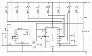
Digital Thermometer 0 100 0°Celsius
Digital Thermometer 0-100.0 ° C is a digital thermometer that operates in mode temperature measurement in Celsius (° C). Digital Thermometer 0-100.0 ° C in this article using the form data processing microcontroller AT89C4051. Temperature sensors used in Digital Thermometer 0-100.0 ° C. This temperature sensor LM35D. Digital Thermometer 0-100.0 ° C. It uses the temperature measurement data viewer in the form of 1 line LCD viewer. Digital Thermometer 0-100.0 ° C. It can display the temperature measurement data with a resolution of 0.1 ° C.
Digital Thermometer 0-100.0 ° C 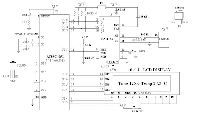
Digital Thermometer 0-100.0 ° C. These temperature sensors make use of LM35D as temperature sensing. In Digital Thermometer 0-100.0 ° C. This temperature sensor measurement data this LM35D (Level Voltage) is then converted into 4-bit binary data using the ADC CA3162. Then the 4-bit data from ADC CA3162 which is a measurement of data if the temperature is in the AT89C4951 microcontroller so that it becomes an operating principle of temperature measurement based on digital thermometers. In the final stage of the Digital Thermometer 0-100.0 ° C. These data digitla adlah appearance temperature measurement, using digital data viewer of the LCD 1 line.
Digital visitor counter
Digital visitor counter is a reliable circuit that takes over the task of counting Number of Persons/ Visitors in the Room very Accurately. When somebody enters into the Room then the Counter is Incremented by one and when any one leaves the room then the Counter is Decremented by One. The total number of Persons inside the Room is displayed on the seven segment displays.The microcontroller do the above job it receives the signals from the sensors, and this signals operated under the control of software which is stored in ROM.
| Digital visitor counter |
| Digital visitor counter |
Monday, November 17, 2014
Preamplifier Circuit Diagram DCF77
DCF77 Preamplifier Circuit Diagram A popular project among microcontroller aficionados is to build a radio-controlled clock. Tiny receiver boards are available, with a pre-adjusted ferrite antenna, that receive and demodulate the DCF77 time signal broadcast from Mainf lingen in Germany.
DCF77 has a range of about 1,000 miles. All the microcontroller need do is decode the signal and output the results on a display. The reception quality achieved by these ready-made boards tends to be proportional to their price. In areas of marginal reception a higher quality receiver is needed, and a small selective preamplifier stage will usually improve the situation further.
The original ferrite antenna is desoldered from the receiver module and connected to the input of the preamplifier. This input consists of a source follower (T1) which has very little damping effect on the resonant circuit. A bipolar transistor (T2) provides a gain of around 5 dB. The output signal is coupled to the antenna input of the DCF77 module via a transformer.
Circuit diagram:
| DCF77 Preamplifier Circuit Diagram |
DCF77 Preamplifier Circuit Diagram The secondary of the transformer, in conjunction with capacitors C4 and C5, forms a resonant circuit which must be adjusted so that it is centered on the carrier frequency. An oscilloscope is needed for this adjustment, and a signal generator, set to generate a 77.5 kHz sine wave, is also very useful. This signal is fed, at an amplitude of a few milli-volts, into the antenna input. With the oscilloscope connected across C4 and C5 to monitor the signal on the output resonant circuit, trimmer C5 is adjusted until maximum amplitude is observed.
It is essential that the transformer used is suitable for constructing a resonant circuit at the carrier frequency. Our proto-type used a FT50-77 core from Amidon on which we made two 57-turn windings. It is also possible to trim the resonant frequency of the circuit by using a transformer whose core can be adjusted in and out. In this case, of course, the trimmer capacitor can be dispensed with. Rainer Reusch Elektor Electronics 2008
Atmel microcontroller Easy Downloader Circuit
Easy Downloader Circuit
Atmel microcontroller series AT89Cxx51 Easy Downloader is one of the downloader that is often used to write data to program the Atmel microcontroller AT89CXX51. Easy Downloader AT89Cxx51 ATMEL microcontroller is using the serial port as a channel of communication with the computer.

Easy Downloader ATMEL Microcontroller AT89Cxx51 can be used to program Atmel AT89CXX51 in parallel. Atmel microcontroller series AT89Cxx51 Easy Downloader is quite simple to make your own because the components necessary to membutanya not complex. Atmel microcontroller series AT89Cxx51 Easy Downloader do not support the serial programming microcontrollers ISP. In the article Easy Downloader ATMEL Microcontroller AT89Cxx51 only displays images Easy Downloader Microcontroller series from Atmel AT89Cxx51 only and are simple.
LM3914 IC based on Simple Battery Tester
This LM3914 IC based on Simple Battery Tester is very simple to explain:
Once the test switch is pushed, the Car battery voltage is supply into a high impedance voltage divider. His function is to divide 12V to 1, 25V (or lower values to reduced values). This solution is much better than enabling the internal voltage regulator set the 12V sample voltage to be feed into the internal voltage divider simply because it cannot regulate 12V if the voltage falls lower (linear regulators only step down). Simply wiring with no change, the regulator provides secure 1, 25V which can be fed into the precision internal resistor cascade to create sample voltages to the internal comparators.
In any case the default establishing let you to determine voltages between 8 and 12V however you can measure even from 0V to 12V setting the offset trimmer to 0 (but i believe that below 9 volt your vehicle would not start). There is a smoothing capacitor (4700uF 16V) it is used to adsorb EMF noises produced from the ignition coil if youre testing the battery during the engine working. Diesel engines would not need it, but i am not sure. If you want more a level graph rather than a bar graph simply disconnect pin 9 on the IC (MODE) from power. The calculations are usually simple (default).
Rain Detector using SCR 106CY
This circuit uses a sensor made of a small piece of circuit board and recorded a simple SCR circuit to detect rain and sound of a bell. The SCR could also be used to activate a relay, light a lamp, or send a signal to a security system.
1. The sensor is a small piece of PC board etched to the pattern showen in the schematic. The traces should be very close to each other, but never touching. A large spiral pattern would also work.
2. Make sure to use a loud buzzer.Sunday, November 16, 2014
Tone control low noise circuit
Tone control or pre-amplifier is an amplifier circuit supporters. Sometimes some of us do not know where a good amplifier, a raft alone and the results are not much different or even the same. Therefore we must know the character of the advantages and disadvantages of each amplifier equipment.
Tone control low noise here does not mean without noise, but noise compared with the lowest tone control on the market, for example Ronica transistor 4, TL-084, TC-2 LM833 etc.
 |
| CSE | Circuit Schematic Electronics |
Jump toexplanation of each component ...
Potensio 1 serves to regulate the intensity / level of the incoming signal is assisted potensio 2 as balance / counterbalance. Potensio 2 is still installed and is usually an optional component. 1-2uF/250V capacitor R1 is actually a brand name,but I prefer to replace it with a 1K resistor / 5% normal for reasons to avoid hum and interference sensitive. R2 R3 while minimizing interruption to adjust the impedance OP-amp 1. R4 and R5 serves to increase the gain of 1.3 times. Pre amplifiers typically use a strengthening standards by 2 times, but by most of us think it has a noise. So I chose the value of 1.3 times, but the most minimal noise signal from the volume is enough to make the lamp light peak.
For low noise ...Cause of noise in op amp 1, apex audio even eliminate this stage. CanThis step is also used as a buffer (jumper R5), the strengthening of a time. Lower values increase the value of R5 or R4 with consequent gains to be less, but remains at a value above 1 times due to input non-inverting path to take, so that the signal and noise can be reduced. R4 can also be replaced with a 10K trimpot and middle leg into the bass range adjuster (bass resonance).
C1 and C6 as a filter to reduce the treble / high frequency of excessive or often called oscillation prevention. R6 is actually an optional component of the impedance a little help customize the system. Ideally the same as the R8 R7 to facilitategive the sign of the gain on potensio panel tone control. C2 and C3 form a series circuit treble filter (high pass filter), its value is greater then the sound that passed the mid. C4 and C5 assisted by R9 and R10 form the low pass filter (filter bass), the greater the value of C is a bass sound that will be missedthe soft / low (maximum of 47nF), the smaller the value of c is the bass signal that is passed will further dip (dig-dig, c4 = c5 = 22nF). This value is suitable for 27-33nF, 47nF instead (depending on taste). Pot 3 & 4 pot set treble and bass levels, the greater the greater the value of this potensio gains (bass & treble including potensio volume). R11 adjusts the output impedance, while the R12 and the red LED indicator that shows if the amplifier Peak has been given a full signal.
15V maximum supply. TL074 IC can, but in designing the PCB, IC can bereplaced with 2x TL072/NE5532/4558.
Car audio amplifier using TDA2003 IC
Easy low power car audio amplifier circuit on TDA 2003. The circuit is Easy to construct. TDA2003 is an integrated radio amplifier from ST Micro electronics that like short circuit protection for all pins, thermal over low harmonic distortion, low cross over distortion etc. In the circuit given here TDA2003 is wired as a mono amplifier operating from a 12V .
Resistors R2 and R3 forms a feedback network that sets the amplifiers gain. C7 input DC de-coupling capacitor and C5 couples the speaker to the amplifiers output. C4 } for improving the ripple rejection C1 and C2 are employed for power filtering. C3 and R1 are used for setting the frequency cut-off. Network comprising of C6 and R4 for frequency stabilization and oscillation.
Resistors R2 and R3 forms a feedback network that sets the amplifiers gain. C7 input DC de-coupling capacitor and C5 couples the speaker to the amplifiers output. C4 } for improving the ripple rejection C1 and C2 are employed for power filtering. C3 and R1 are used for setting the frequency cut-off. Network comprising of C6 and R4 for frequency stabilization and oscillation.
Notes.
- Assemble the circuit on a good quality PCB.
- Heat sinks are necessary for both ICs.
- The circuit can be operated from 12V DC.
- S1 is the ON/OFF switch.
Saturday, November 15, 2014
FLASHER CIRCUIT USING NE 555
Flashing circuits are very interesting. They grab your attention and can be used in many applications. They consume very little energy and a single cell can last as long as 12 months. You can flash globes, LEDs and pulse all types of devices such as motors, solenoids and piezo diaphragms. In this discussion we will cover a number of interesting "oscillator circuits." They can be adapted for other applications - but to do this you have to know how they work. This is not easy as most of them are quite complex. In fact oscillator circuits are one of the most difficult circuits to understand. But if you read the text, everything will become clear.

Circuit Description
This is the circuit diagram of lamp flasher operated from mains. By this you can flash up to 200 Watt lamps at rates determined by you. IC NE555 is wired as an astable multivibrator for producing the pulses for flashing the lamp. The flashing rate can be set by the value of resistors R2 & R3.
Diodes D1 & D2 provides a half wave rectified regulated supply for the IC. Transistor T1 is used to drive triac and triac BT136 for driving the load. Resistor R4 limits the base current of Q1.
Flashing Circuit Diagram & Parts List
Notes
- Assemble the circuit on a good quality PCB or common board.
- Connect a 100K pot instead of R2 if you need frequent changes in rate.
- Many parts of the circuit are live with potential shock hazards. So please be careful.
- As usual use an IC holder for mounting the IC.
Friday, November 14, 2014
SENSITIVE OPTICAL BURGLAR ALARM
This optical burglar alarm uses two 555 timer ICs (IC1 and IC2). Both the ICs are wired as astable multivibrators. The first astable multivibrator built around IC1 produces low frequencies, while the second astable multivibrator built around IC2 produces audio frequencies.General-purpose Darlington photo-transistor T1 is used as the light sensor. To increase the sensitivity of the circuit, NPN transistor T2 is used.
Place phototransistor T1 where light falls on it continuously. Phototransistor T1 receives light to provide base voltage to transistor T2. As a result, transistor T2 conduct to keep reset pin 4 of IC1 at low level. This disables the first multivibrator (IC1) and hence the second multivibrator (IC2) also remains reset so the alarm (LS1) does not sound.
Circuit Diagram

When light falling on Darlington phototransistor T1 is obstructed, transistor T2 stops conducting and reset pin 4 of IC1 goes high. This enables the first multivibrator (IC1) and hence also the second multivibrator (IC2). As a result, a beep tone is heard from speaker LS1. The beep rate can be varied by using preset VR1, while the output frequency of IC2 can be varied by using another preset VR2.
This circuit works off a simple 6V-12V DC power supply.
Parts List
Resistors (all ¼-watt, ± 5% Carbon unless stated otherwise)
R1, R5 = 1 KΩ
R2 = 100 KΩ
R3 = 4.7 KΩ
R4 = 10 KΩ
VR1 = 1 MΩ
VR2 = 100 KΩ
Capacitors
C1 = 1 µF/16V
C2 = 0.01 µF
C3 = 0.047 µF
C4 = 0.01 µF
C5 = 47 µF/25V
Semiconductors
IC1, IC2 = NE555
T1 = 2N5777 Photo Transistor
T2 = BC547
LED1 = RED LED
Miscellaneous
LS1 = 8Ω / 0.5W
LINE FOLLOWER ROBOT USING 8051
Line follower robots were one of the earliest automatic guided robots. They are able to follow a line marked on a contrasting background, usually a black line on a white surface or a white line on a black surface. Usually the line follower robot works on a closed loop feedback algorithm where the feedback from the line sensor is used by the controller for correcting the path of the robot. The sensors are usually LED/LDR, LED/Photodiode or LED/Phototransistor pairs and the controller is an electronic circuit which executes the desired feedback algorithm. Gear motors are used for driving the robotic wheels.
The line follower robot presented here is designed to follow a black line on a white background. It has a pair of sensors (LED / LDR) and works on a simple “align robot on center of the line algorithm”. Actually you does not need a microcontroller for implementing such a simple robot. A set of comparators and a motor driver circuit will happily do the job. But I am using the microcontroller just to demonstrate the technology. Also this project serves as a platform for advanced line follower robots which works on complex algorithms. AT89S52 from Atmel is the microcontroller used here.
Sensor
The sensor part consists of a set of LED / LDR pairs for the left side and right sides. These LED / LDR pairs detect the black line on the white surface on which the robot is supposed to roam. The LDR has an inverse relationship between its resistance and the light falling on it. When a particular LED / LDR pair is above the white surface the reflected light falls on the LDR and its resistance drops, conversely when the LED / LDR pair is above the black line, its resistance rises. This variation in resistance of the LDRs are used to asses the orientation of the line follower robot in the X-Y plane. The figure shown below depicts the sensor circuit.

In the circuit, resistors R1 and R2 limits the current through the illuminating LEDs D1 and D2. Resistors R3, R5 and R6, R8 forms a voltage divider network together with the corresponding LDRs. The output of the sensor circuit is taken from the points labelled A and B in the circuit diagram.The table below shows the voltage at nodes A and B for the possible orientations of the sensor module.

Comparator Circuit
The job of the comparator circuit is to convert analog voltage output of the sensor into a digital format for the microcontroller to read. The comparator circuit is built around opamp IC LM324 (IC1). LM324 is a general purpose quad opamp which can be operated from a single supply. Out of the four comparators inside LM324, only two are used here. One for the left side and the other for the right side. Circuit diagram of the comparator section is shown in the figure below.

Preset resistor R10 and R11 are used to set the 1V reference for the left and right comparators respectively. Output from the left and right sensors (node A and B) are connected to the non inverting input on the left and right comparators. Output of the left comparator is connected to P1.o of the microcontroller and output of the right comparator is connected to P1.1 of the microcontroller. Both comparators are wired in non inverting mode and the table given below shows their output voltage with respect to the possible input voltage combinations.

Microcontroller (AT89S52)
The task of the microcontroller here is to control the left and right motors according to the feedback signals from the left and right comparators so that the robot remains on the correct path (the black line). The logic executed by the microcontroller for keeping the robot in track is illustrated in the table below.

Motor Driver Circuit
The job of the motor driver circuit is to drive the motors according to the output signals from the microcontroller. The motor driver circuit is based on ULN2003A IC. ULN2003A is a high current (500mA), high voltage (50V) darlington array consisting of seven darlington pairs with common emitter and open collector. Out of the seven channels available in the IC,only two are used here. One for the left channel and one for the right channel. Schematic of the motor driver circuit is shown in the figure below. The operation of ULN2003 is very simple to explain. When a particular input line (say pin 1) is made high the corresponding output line (pin 16 goes low) and vice versa.

Capacitors C4 and C5 isolates the remaining parts of the circuit from the electric interference produced by the motor. The back emf voltage produced when motor is switched and the voltage spikes due to arcing of brushes mainly accounts for the above said electrical interference. These capacitors are very essential and without them you can expect sudden crashes from the microcontroller side.
Complete Circuit Diagram

Switch S1, capacitor C3 and resistor R9 forms a debouncing reset circuit for the microcontroller. Capacitors C1, C2 and 12MHz crystal X1 are associated with the microcontroller’s clock circuit. R12 and R13 are pull-up resistors. Remaining sections of the circuit were explained already.
Program
ORG 000H // origin
MOV P1,#00000011B // sets port 1 as input port
MOV P0,#00000000B // sets port 0 as output port
BACK : MOV P0,#00000011B // starts both motors
JB P1.0, LABEL1 // branches to LABEL1 if left sensor is ON
CLR P0.0 // stops left motor
SETB P0.1 // runs right motor
ACALL WAIT1 // calls WAIT1 subroutine
SJMP BACK // jumps back to the BACK loop
LABEL1 : JB P1.1, LABEL2 // branches to LABEL2 if right sensor is ON
SETB P0.0 // runs left motor
CLR P0.1 // stops right motor
ACALL WAIT2 // calls WAIT2 subroutine
SJMP BACK // jumps back to the BACK loop
LABEL2 : SJMP BACK // jumps back to the BACK loop
WAIT1 : JNB P1.0,WAIT1 // waits until robot is back from rightward deviation
RET // returns from WAIT1 subroutine
WAIT2 : JNB P1.1,WAIT2 // waits until robot is back from leftward deviation
RET // returns from WAIT2 subroutine
END // end statement
About the Program
The first part of the program initializes Port 1 as input port and Port 0 as output part. After this, both motors are started so that the robot goes straight. Then the programs checks whether there is a deviation to right. If there is a deviation to right, the program stops left motor and runs right motor and waits until the robot comes back from the deviation. When the robot is back on line again, both motors are started.
If there is no deviation to right, the program checks for a deviation to left. If there is a deviation to left, left motor is stopped and right motor is activated. This condition is maintained until the robot is back on track. When the robot is back on track again, both motors are started. Lastly if there is no deviation to left or right, both motors are kept ON.
Notes
- A 6V battery can be used for powering the circuit even though the power supply shown in the circuit diagram is 5V DC.
- For setting up the robot, place the robot on the line so that both the sensor pairs point on white and the black line goes in between them. Then adjust preset resistors R10 and R11 so that the LEDs D3 and D4 glows.
- Sensor LEDs D1 and D2 are ultra-bright green LEDs.
- OPAMP output LEDs D3 and D4 are general purpose, miniature, yellow LEDs.
- Sensor LDRs R4 and R7 are general purpose LDRs.
Subscribe to:
Posts (Atom)