Friday, October 31, 2014
Operational Amplifiers with Power Supply
The single feed mode has become very important in systems powered from a single power supply, because it reduces the cost of circuits with operational amplifiers and also makes it easier to use on mobile devices. In this series of articles will look at various ways that can power amplifiers circuits using operational amplifiers with single power supply (single rail).
The diagram of a sound amplifier, which operates with a single power supply shown in Figure 16. In this circuit one end of the signal source connected to the right input terminal of the operational amplifier, and the other end connected to the bias voltage VBias.
The load resistance (RL) and R1 also associated with the bias voltage. The voltage at the right input terminal, VP, is equal to:
The voltage at the reverse input terminal VN, is equal to:
The diagram of a sound amplifier, which operates with a single power supply shown in Figure 16. In this circuit one end of the signal source connected to the right input terminal of the operational amplifier, and the other end connected to the bias voltage VBias.
The load resistance (RL) and R1 also associated with the bias voltage. The voltage at the right input terminal, VP, is equal to:
Vp = VBias + Vin
The voltage at the reverse input terminal VN, is equal to:
VN = VD + VP but because,
Vd = 0 we have:
VN = VP = Vin + VBias
without an input signal
Vin = 0, so therefore
Vn = Vp = VBias
Vd = 0 we have:
VN = VP = Vin + VBias
without an input signal
Vin = 0, so therefore
Vn = Vp = VBias
Figure 16. Amplifier with single power supply.
Figure 17. Input and output waveforms of the amplifier of Figure 16.
The bias voltage (VBias) is typically equal to half the voltage of the power supply. The output voltage of this amplifier can be calculated as follows:
The current I1, which flows through the resistor R1, is approximately equal to the current I2, which flows through the resistor R2, and thus I1 = I2. The current flowing through R1 is equal to the difference voltage across R1 divided by the value of R1, ie

In this circuit VB is the voltage applied to the right end of R1, and VA is the voltage applied to the left end of R1.
From the figure 16 we see that:
VB = VP but VP = VBias + VIN, thus:
VB = VBias + VIN
We also have VA = VBias so:

Similarly, the current I2 flowing through the resistor R2, is equal to the difference voltage across the R2.
i.e. VR2 = VO - VB divided by the value of R2
We also have VB = VBias + VIN, thus:

Figure 18a. AC amplifier with simple power supply.
Since I1 = I2, we obtain:

Rearranging we get:


So in the absence of an input signal, ie when VIN = 0, the above equation becomes

or VO = VBias
So in the absence of an input signal, the input terminals and the output terminal of the operational amplifier have the same voltage (VBias).
If an input voltage 2 volts peak to peak, is applied to the amplifier shown in Figure 16, R1 = R2, and VCC = 10V, then when the input signal is at the positive peak value of +1V, the output voltage will be:


When the input signal changes is at its highest negative value -1V, then the output voltage equals:

So when the input signal changes from -1V to +1V, the output voltage varies from +3V to +7V.
Figure 17 shows waveforms of the input and output. Notice that the first term in equation 1 represents the voltage gain of a conventional amplifier using a double power supply. The voltage gain is given by the following relationship:

In a conventional non-inverting amplifier, which operates with double supply, the bias voltage VBias is equal to 0 volts, and the output voltage is given by the following equation:

300 Watt Power Amplifier Elektor 11 1995

There are several starting points to the design of a power amplifier: pure hi-fi without any compromise; simplicity and reliability; high output power. The design of the present amplifier is a mixture of these. The result is a unit that does not use esoteric components, is not too complex, and is fairly easily reproduced. In fact, it could well be named a Hi-fi public address amplifier.
There will be a few eyebrows raised at the power output of 300 watts (into 4Ohm); it is true, of course, that in the average living room 30–40 W per channel is more than sufficient. However, peaks in the reproduced music may have a power of 10–20 times the average level. This means that some reserve power is desirable. Also, there are loudspeakers around with such a low efficiency that a lot more than 30–40W is needed. And, last but not least, there are many people who want an amplifier for rooms much larger than the average living room, such as an amateur music hall.
 Fig. 1. With the exception of an IC at the input, the circuit of the PA300 amplifier is conventional.
Straightforward designSince every amplifier contains a certain number of standard components, the circuit of Fig.1 will look pretty familiar to most audio enthusiasts. Two aspects may hit the eye: the higher than usual supply voltage and the presence of a couple of ics. The first is to be expected in view of the power output. One of the ics is not in the signal path and this immediately points to it being part of a protection circuit. What is unconventional is an IC in the input stage. Normally, this stage consists of a differential amplifier followed by a voltage amplifier of sorts, often also a differential amplifier, to drive the predriver stages. In the PA300, the entire input stage is contained in one ic, a Type NE5534 (IC1).
The internal circuit of IC1 is shown in the box on further on in this article. It may also be of interest to note that the NE5534 is found in nine out of every ten cd players(as amplifier in the analogue section). This is reflected in its price which is low. Its only drawback is that its supply voltage is far below that of the remainder of the amplifier.
This means an additional symmetrical supply of ±15 V. Moreover, it restricts the drive capability of the input stage. The supply requirement is easily met with the aid of a couple of zener diodes and resistors. The drive restriction means that the amplifier must provide a measure of voltage amplification after the input stage.
Circuit description
The input contains a high-pass filter, C5-R3 and a low-pass filter, R2-C6. The combination of these filters limits the bandwidth of the input stage to a realistic value: it is not necessary for signals well outside the audio range to be amplified – in fact, this may well give rise to difficulties.
Opamp IC1 is arranged as a differential amplifier; its non-inverting (+) input functions as the meeting point for the overall feedback. The feedback voltage, taken from junction D7-D8, is applied to junction R4-R5 via R9. Any necessary compensation is provided by C9, C12 and C14. The voltage amplification is determined by the ratio R9:R5, which in the present circuit is x40.
The output of IC1 is applied to drive stages T1 and T3 via R6. These transistors operate in Class A: the current drawn by them is set to 10 mA by voltage divider R10- R13 and their respective emitter resistors. Their voltage and current amplification is appreciable, which is as required for the link between the input and output stages. The output amplifier proper consists of drive stages T6 and T7 and power transistors T8, T9, T14, T15. which have been arranged as symmetrical power darlingtons. Because of the high power, the output transistors are connected in parallel. The types used can handle a collector current of 20 A and have a maximum dissipation of 250 W.
The output stages operate in Class AB to ensure a smooth transition between the n-p-n and p-n-p transistors, which prevents cross-over distortion. This requires a small current through the power transistors, even in the absence of an input signal. This current is provided by zener transistor T2, which puts a small voltage on the bases of T6 and T7 so that these transistors just conduct in quiescent operation. The level of the quiescent current is set accurately with P1.
To ensure maximum thermal stability, transistors T1–T3 and T6–T7 are mounted on and the same heat sink. This keeps the quiescent current within certain limits. With high drive signals, this current can reach a high level, but when the input signal level drops, the current will diminish only slowly until it has reached its nominal value.
Diodes D7, D8 protect the output stages against possible counter voltages generated by the complex load. Resistor R30 and capacitor C17 form a Boucherot network to enhance the stability at high frequencies. Inductor L1 prevents any problems with capacitive loads (electrostatic loudspeakers). Resistor R29 ensures that the transfer of rectangular signals are not adversely affected by the inductor.
Protection circuitsAs any reliable amplifier, the PA300 is provided with adequate protection measures.
These start with fuses F1 and F2, which guard against high currents in case of overload or short-circuits. Since even fast fuses are often not fast enough to prevent the power transistors giving up the ghost in such circumstances, an electronic short-circuit protection circuit, based on T4 and T5, has been provided. When, owing to an overload or short-circuit, very high currents begin to flow through resistors R25 and R27, the potential drop across these resistors will exceed the base-emitter threshold voltage of T4 and T5. These transistors then conduct and short-circuit or reduce drive signal at their bases. The output current then drops to zero. If a direct voltage appears at the output terminals, or the temperature of the heat sink rises unduly, relay Re1 removes the load from the output. The loudspeakers are also disconnected by the relay when the mains is switched on (power-on delay) to prevent annoying clicks and plops.
The circuits that make all this possible consist of dual comparator IC2, transistors T10–T13, and indicator diodes D13 and D14. They are powered by the 15 V line provided by zener diode D10 and resistor R42.
The ac terminal on the PCB is linked to one of the secondary outputs on the mains transformer. As soon as the mains is switched on, an alternating voltage appears at that terminal, which is rectified by D12 and applied as a negative potential to T12 via R50. The transistor will then be cut off, so that C20 is charged via R36 and R44. As long as charging takes place, the inverting (+) input of comparator IC2b is low w.r.t. the non-inverting (–) input. The output of IC2b is also low, so that T13 is cut off and the relay is not energized. This state is indicated by the lighting of D13. When C20 has been charged fully, the comparator changes state, the relay is energized (whereupon D13 goes out) and the loudspeakers are connected to the output. When the mains is switched off, the relay is deenergized instantly, whereupon the loudspeakers are disconnected so that any switch-off noise is not audible.
The direct-voltage protection operates as follows. The output voltage is applied to T10 and T11 via potential divider R32-R34. Alternating voltages are short-circuited to ground by C18. However, direct voltages greater than +1.7 V or more negative than –4.8V switch on T10 or T11 immediately. This causes the +ve input of IC2a to be pulled down, whereupon this comparator changes state, T13 is cut off, and the relay is deenergized. This state is again indicated by the lighting of D13.
Strictly speaking, temperature protection is not necessary, but it offers that little bit extra security. The temperature sensor is R39, a ptc (positive temperature coefficient) type, which is located on the board in a position where it rests against the rectangular bracket. Owing to a rising temperature, the value of R39 increases until the potential at the –ve input of IC2a rises above the level at the +ve input set by divider R45-R46, whereupon the output of IC2a goes low. This causes IC2b to change state, whereupon T13 is cut off and the relay is deenergized. This time, the situation is indicated by the lighting of D14. The circuit has been designed to operate when the temperature of the heat sink rises above 70 °C. Any relay clatter may be obviated by reducing the value of R48.
The terminal marked CLIP on the PCB is connected to the output of IC1 via R31. It serves to obtain an external overdrive indication, which may be a simple combination of a comparator and LED. Normally, this terminal is left open.
Power supply
As with most power amplifiers, the ±60 V power supply need not be regulated. Owing to the relatively high power output, the supply needs a fairly large mains transformer and corresponding smoothing capacitors—see Fig. 2. Note that the supply shown is for a mono amplifier; a stereo outfit needs two supplies.

Fig. 2. The power supply is straightforward, but can handle a large current. Voltage acserves as drive for the power-on delay circuit.
The transformer is a 625 VA type, and the smoothing capacitors are 10 000 µF, 100 V electrolytic types. The bridge rectifier needs to be mounted on a suitable heat sink or be mounted directly on the bottom cover of the metal enclosure.. The transformer needs two secondary windings, providing 42.5 V each. The prototype used a toroidal transformer with 2x40 V secondaries. The secondary winding of this type of transformer is easily extended: in the prototype 4 turns were added and this gave secondaries of 2x42.5 V.
The box Mains power-on delay provides a gradual build-up of the mains voltage, which in a high-power amplifier is highly advisable. A suitable design was published in 305 Circuits (page 115).
The relay and associated drive circuit is intended to be connected to terminal ac on the board, where it serves to power the power-on circuit. If a slight degradation of the amplifier performance is acceptable, this relay and circuit may be omitted and the PCB terminal connected directly to one of the transformer secondaries.

Fig. 3. Component layout of the printed-circuit board for the 300 W power amplifier.

Fig. 4. Track layout of the printed-circuit board for the 300 W power amplifier.
ConstructionBuilding the amplifier is surprisingly simple. The printed-circuit board in Fig. 4 is well laid out and provides ample room. Populating the board is as usual best started with the passive components, then the electrolytic capacitors, fuses and relay. There are no difficult parts.
Circuits IC1 and IC2 are best mounted in appropriate sockets. Diodes D13 and D14 will, of course, have to be fitted on the front panel of the enclosure and are connected to the board by lengths of flexible circuit wire. Inductor L1 is a DIY component; i consists of 15 turns of 1 mm. dia. enamelled copper wire around R29 (not too tight!). Since most of the transistors are to be mounted on and the same heat sink, they are all located at one side of the board. However, they should first be fitted on a rectangular bracket, which is secured to the heat sink and the board—see Fig. 3. Note that the heat sink shown in this photograph proved too small when 4 Ohm loudspeakers were used. With 8 Ohm speakers, it was just about all right, but with full drive over sustained periods, the temperature protection circuits were actuated. If such situations are likely to be encountered, forced cooling must be used. As already stated, temperature sensor R39 should rest (with its flat surface) against the rectangular bracket. On the board, terminals A and B terminals to the left of R39 must be connected to A and B above IC2 with a twisted pair of lengths of insulated circuit wire as shown in Fig. 3. The points where to connect the loudspeaker leads and power lines are clearly marked on the board. Use the special flat AMP connectors for this purpose: these have large-surface contacts that can handle large currents. The loudspeaker cable should have a cross-sectional area of not less than 2.5 mm2.
FinallyHow the amplifier and power supply are assembled is largely a question of individual taste and requirement. The two may be combined into a mono amplifier, or two each may be built into a stereo amplifier unit. Our preference is for mono amplifiers, since these run the least risk of earth loops and the difficulties associated with those. It is advisable to make the 0 of the supply the centre of the earth connections of the electrolytic capacitors and the centre tap of the transformer.
The single earthing point on the supply and the board must be connected to the enclosure earth by a short, heavy-duty cable. This means that the input socket must be an insulated type. This socket must be linked to the input on the board via screened cable.
To test the amplifier, turn P1 fully anticlockwise and switch on the mains. After the output relay has been energized, set the quiescent current. This is done by connecting a multimeter (direct mV range) across one of resistors R25–R28 and adjusting P1 until the meter reads 27 mV (which corresponds to a current of 100 mA through each of the four power transistors). Leave the amplifier on for an hour or so and then check the voltage again: adjust P1 as required.
Watch LG G R be the new clock screen rounder than the Moto 360
The Motorola Moto 360 has made big news due to be the first smart watch with Android Wear having a circular screen, but it seems that this is not the only watch to have this feature in the coming months.
The official account of LG Mobile Global YouTube posted a video called "LGs New Wearable" (New LG portable devices ", which could carry the name of LG G Watch R, reports Engadget.
The device images of different faces of a watch and makes it clear that it would be the first intelligent clock completely circular screen. We recall that the Moto 360 has a round screen, but the bottom has a light sensor that takes away a part of the screen.
At the moment no concrete details on how you could compare the LG G Watch R versus LG G Watch with square screen with the Moto 360 However, the video promises we know about the new watch known for IFA 2014, an event that begins on September 5.
It is possible that the LG G Watch R goes on sale while the curve G Watch screen remains on the market, because different forms may be of interest to different audiences.
Thursday, October 30, 2014
DIN Valve Connectors for Solenoids
Solenoids are versatile components used for various industrial purposes. Theyre quite simple, consisting of a coil and a spring-loaded plunger within a suitable housing. This simple arrangement is used in a variety of industrial automation procedures, including complex machine building, pneumatic valves, hydraulic valves, robotics, pressure switches, transducers and solenoid valves. Real-world applications extend to on-vehicle cranes, lifting equipment and even garbage trucks.

Molex make external-threaded DIN Valve Connectors that have excellent sealing properties along with superior cable retention. This increases the performance and reliability of their solenoids. By simplifying the manufacturing processes, Molex reduces the overall applied costs for all types of solenoids used in electromagnetic, pneumatic and hydraulic devices.
 Molex has provided several features and benefits in their simple but innovative design -
• The external nut is ergonomically designed for greater and consistent torque providing uniform sealing between connector and cable. The cable retention force is now 115%, offering improved reliability.
• The customers inventory is reduced, since PG9, PG11 and cables of outer diameter up to 9mm can be accommodated.
• Errors are eliminated, as an incorrectly-sized installer cannot be used. The front gasket is integrated and self-retaining within the housing, preventing it from being misplaced during assembly.
• Handling, wire routing and speed of assembly is increased by via the 30% increase in internal volume because of external nut design. Speed of assembly is further reduced since the connector is supplied disassembled.
• Plus / minus screwheads enable air tools to be used for volume production. In the field an operator can use either a flat or a Phillips-head screwdriver.
Goldmund Mimesis 3 schmatic

Gas SENSOR MODULE
The SEN-1327 LPG chatter Sensor Module is designed to enable LPG detection interface to Microcontroller devoid of ADC Channels. It allows to determine while a set LPG chatter level has been reached otherwise exceeded. Interfacing with the sensor module is made through a 4-pin SIP title and requires lone I/O pin from the host microcontroller.
The onboard microcontroller provide preliminary heating interval bearing in mind powerup and therefore starts to meassure LPG sensor output.If it found the LPG contents exceeding setted estimate, it self-control tell the Host controller by pulling the Output Pin to elevated and Starts to blink a onboard status LED. The sensor module is for the most part intended to provide a revenue of comparing LPG sources and being able to prearranged an alarm limit whilst the source becomes unnecessary.
SEN1327 pins configuration and photo

SEN-1327 module skin texture
- Uses the MQ-6 LPG gab Sensor
- undemanding SIP interface
- Compatible with largely microcontrollers
- Onboard Status and Power LED
- Onboard Pot representing threshold setting
- On board microcontroller
0 3 to 1 5V LED Flashlight Circuit Diagram
Its a little wisp of a circuit that allows you to drive a blue or white LED from a low voltage. Normally, if you want to light up a blue or white LED you need to provide it with 3 - 3.5 V, like from a 3 V lithium coin cell. But a 1.5 V battery like a AA cell simply will not work. But using the Joule Thief, it works like a charm. Not only does it work with a brand new battery, but it works until the battery is nearly dead-- down to 0.3 V. Thats well below the point where your other toys will tell you the battery is dead, so it can steal every last joule of energy from the battery (hence the name). To learn how to make one, watch the video, which is available in a variety of formats.
0.3 to 1.5V LED Flashlight Circuit Diagram
0.3 to 1.5V LED Flashlight Circuit Diagram

Wednesday, October 29, 2014
Collection Scheme Audio Power Amplifier High Power MOSFETs

200W Audio Amplifier with Mosfet BUZ905P-BUZ900P
This project is develop from the MOSFET Power amplifier 100W that posted which it take to use in many activity such as Guitar amp,Mic,or Home theater and you will be to apply it.As many people prefer because of its robustness MOSFET legendary. Altronics had a MOSFET amplifier with 200W, the product in a 4Ω, and we have decided to take a look at is.
It turns out that on the basis of the Pro One “, as described above, even if this version of Altronics and to the various MOSFETs. He has a rated output of 140W to 200W into 4Ω and 8W. Frequency range of 1 dB 20Hz up to 80kHz (Fig. 1). THD is less than 0.1% at full power (Fig. 2) and signal to noise ratio when compared to 200W is better than -100 dB unweighted.

Output power (RMS ):… 140W into 8 ohms, 200W into 4 ohms
Frequency Response:. 20Hz – 80kHz-1dB points (see Figure 1)
Input sensitivity: ………… 830mV for 200W into 4 ohms
Distortion: … <0.1% (20 Hz – 20 kHz) (see Fig.2)
Signal-to-Noise Ratio:. > 102dB unweighted, 105dB A-weighted with respect to 200W into 4 ohms
Stability :…………………….. Unconditional
Originally, the “Pro Series One” was developed by Hitachi MOSFET A-3 metal containers. They are no longer available, and their counterparts from plastics are very difficult to obtain. Altronics on this situation and have essentially the same circuits designed for Plastic MOSFET corresponds Exicon by the United Kingdom. This required a re-design of the computer, so that all MOSFET and the pilot for all transistors on a plate are vertically mounted on the radiator.
Besides the use of plastic in the power transistors, which greatly simplifies the assembly of the metal in comparison with A-3 power transistors, have Altronics spring clips in the proximity of the pairs of transistors, so things were still simple. The spring clips, just what the voltage for transistors and there is no harm in a transistor due to struggle more screws.
The heat sink is a black anodized aluminum extrusion with fins on one side. It measures 300 mm long and has a lid that a 80mm fan cooled 24V DC. The fan runs constantly, which means that the radiator is always cool (or at least slightly above the ambient temperature).
100W Audio Amplifer Circuit With MOSFET IRFP240
MOSFET amplifier with MOSFET for your build in electronic hobby.
I would like to show you here a basic MOSFET amplifier or power Amp which Output power is plus/minus 100 Watt/RMS with
8 Ohms or ohter plus/minus 160 Watts /RMS with 4 ohms.
Regarding this circuit simplicity, The distortion is plus/minus 0.1 %.
For band-width -3 db(decibel) is gain for 4 Hz to 96 Khz, it is limited by C1, R1, C2 and R2.
In the two transistors are T1 and T2 makes a first differential stage part, So,current source(I) of +/- one mA is set with resistor R3.
For the upgraded project, The current source(I) is more efficient in stability. Coil P1 allows a fine tuning of direct current voltage at amplifier’s output. Place the Coil P1 with it’s half value for first power up, then turn it slowly for a lowest DC output voltage. Use a first quality compoment.
Electronic Part
C1 = 2,2 µF MKP, MKT 100 V
C2 = 330 pF céramique 50 V
C3 = 100 nF MKP, MKT 100 V
C4 = 100 µF 40 V électro-chimique
C5, C6 = 18 pF céramique 50 V
C7 = 100 nF MKP, MKT 250 V (C8 = 47 µF 100 V)
R1, R3 = 47 K (R3 = 330 -> 470 Ohms)
R2 = 2K2
R4, R5 = 3K9
R6 = 1 K
R7 = 27 K
R8, R9, R11 = 100 ohms
R10 = 10 K
R12, R13 = 470 ohms
R14, R15 = 0.33 ohms 5 watts
R16 = 10 ohms 3 watts (R17 = 1 K R18, R19 = 10K)
T1, T2, T9,T10 = 2SD756A,2SD716A, BC556B (attention au brochage différent – take care for pin layout)
T7 = IRFP240, 2SK1530, 2SJ162, BUZ900DP, BUZ901DP (attention au brochage different – take care for pin layout : GDS GSD)P1 = 100 ohms (25 tours – 25 turns)
230W Audio Amplifer Circuit With MOSFET IRFP240,9240

230 W MOSFET Audio Amplifer Circuit Here is simple LED-power audio amplifier circuit with MOSFET amplifier TL071C and 2 may be up to 45 W into 8 ohms.
The scheme is at the request SILICONIX and the voltage change of 2 serial resistances from suppliers operating voltage amplifier driver was inserted.
MOSFET must be mounted on at least one condenser 1K / W.
Amplifier efficiency is 70%, the reduction in the frequency distortion in more than 0.2% at 20 Hz at 8 ohms and 10W.
With a supply voltage in the range of + – 30V, can supply audio amplifier MOSFET 45W into 8 ohms and 70W into 4 ohms.
Remember that the sound amplifier is short, so all you can check the radio button is protected, whether the speaker is connected.
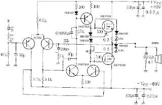
400Watt Audio Power Amplifier with Mosfet BUZ902DP

To view the full performance of each supply transformer should be evaluated at 40VAC – 0 – 40VAC at 640VA.
Unlike many models of capacitors is a reservoir to supply the peak currents, I prefer the power transformer in a much faster transient. BUZ902DP Although the specifications are rather modest,
if they can hear you now to experience a large reserve of power available and never any reason to worry that something to do than drive a large number of amplifiers aloud. You do not hear nothing but the truth without distortion at all levels, and I can assure you that this amplifier is required to provide the best features coupled.
800 Watt Audio Amplifer circuit with MOSFET

The audio power amplifier ideal for home user or PA work or for use as a general-purpose subwoofer or hi-fi amplifier. There are many people like to prefer MOSFET as their legendary ruggedness.
This circuit project had the Mosfet amplifier module which produced 800 Watt into 4 Ohm speaker load and so we decided to take a look it.
It was turned out to be based on the “Pro Series One” as mentioned above, although this version by Altronics has had derated and adapted to different MOSFET. It has a power output rate with 700W into 8W and 800W into 4 Ohm. For frequency response is within 1dB from 20Hz to 80kHz. Total harmonic distortion is rated at less than 0.1% up to full power and signal-to-noise ratio with respect to 800W is better than 100dB unweighted.
For circuit using MOSFET number BUZ902DP ,BUZ907DP which is popula take to build amplifer, If you see the circuit ,It seen 2 same circuits in the project which one circuit can gen power output at 400 Watt.
1000W MOSFET Audio Amplifier Circuit

So,I would like to show you the 1000Watts MOSFET amplifier circuit for your build sound system.
Click the picture left side to open the Circuit in PDF file.
I include full schemaatic chart and film; pattern of the 1000-watt amplifier and a step by step instructions for setting the construction of the amplifier is a true full 1000 watts per channel.
I have been building and playing very well goood can drive a 18 Bring with inch subwoofer dual magnet high performance at UA smooth clear and crisp sound that I used for outdoor event and mobile services when building you will, said this amp I can only contact me gave my email Mail on how to get this project … I assure you his powerful …. You could, but I have to return it a full program of 20 band equalizer can be difficult to find on the net …
8051 Microcontroller projects
Microcontroller projects using the AT8951, 11.0592 MHz crystal or 12 MHz, the capacitor connected to pin no.9 of the IC chip is a reset to the initial unconditioned. The length of reset depending on the size of capacitor and resistor.

Download 8051 microcontroller projects, datasheet, and instruction in assembly language. You can download the form or open a PDF file below via docstoc.
>>>> AT89S51 datasheet
A mini roulette system
A mini roulette circuit, as soon as the switch S1 the output next to pin 1 of the IC1a the voltage is “sharp”,The oscillator circuit output IC2b, IC2c work out.alarm clock pulse generator fed to IC3, a voltage “high” output to the output pins 3, 11, and pin 12 of the IC3, the LED1-LED10 light track sequence. Section LED11 parade high - low instant. The output of pin 3, 2, 4, 7, 10, of IC3 represented by high points,Output pins 1, 5, 6, 9, 11 as a replacement for of the IC3 with the low points.The roll-over prize meant for the LED12.The IC1b, IC2a and IC2d like controls.

Resistor R2 and capacitor C1 determine the punctuation mark of the output “excessive” output from pin 1 of the IC1a. The capacitor C1 through R2. as you press the switch and the voltage shelve across C1 spirit little by little swell until the greatest level. It will reset the flip fall down IC1a suit the output next to pin 1 is “low”. And the oscillator output circuit to pause working, but at hand are a number of LED illumination are pending, it might exist to facilitate we close up being the LED. So carry out not concern, it desire switch a only some time.since, particular a schedule punctuation mark with the aim of the R2 and C1. The diplomacy are compulsory to keep a 6-volt power supply. If distorted is 9 volts, requisite try representing security reasons.
Automatic Switch For Audio Power Amplifier
Circuit of an automatic switch for audio power amplifier stage is presented here. The circuit uses stereo preamplifier output to detect the presence of audio to switch the audio power amplifier on only when audio is present. The circuit thus helps curtail power wastage. IC1 is used as an inverting adder. The input signals from left and right channels are combined to form a common signal for IC2, which is used as an open loop comparator. IC3 (NE556) is a dual timer. Its second section, i.e., IC3(b), is configured as monostable multivibrator. Output of IC3(b) is used to switch the power amplifier on or off through a Darlington pair formed by transistors T1 and T2. IC3(a) is used to trigger the monostable multivibrator whenever an input signal is sensed.
Circuit diagram:
Automatic Switch For Audio Power Amplifier Circuit Diagram
Under ‘no signal’ condition, pin 3 of IC2 is negative with respect to its pin 2. Hence the output of IC2 is low and as a result output of IC3(a) is high. Since there is no trigger at pin 8 of IC3(b), the output of IC3(b) will be low and the amplifier will be off. When an input singal is applied to IC1, IC2 converts the inverted sum of the input signals into a rectangular waveform by comparing it with a constant voltage which can be controlled by varying potentiometer VR1. When the output of IC2 is high, output pin 5 of IC3 goes low, thus triggering the monostable multivibrator. As soon as the audio input to IC1 stops, pin 5 of IC3 goes high and pin 1 of IC3 discharges through capacitor C3, thus resetting the monostable multivibrator.
Hence, as long as input signals are applied, the amplifier remains ‘on.’ When the input signals are removed, i.e., when signal level is zero, the amplifier switches off after the mono flip-flop delay period determined by the values of resistor R8 and capacitor C3. If no input signals are sensed within this time, the amplifier turns off—else it remains on. Power supply for the circuit can be obtained from the power supply of the amplifier. Hence, the circuit can be permanently fitted in the amplifier box itself. The main switch of the amplifier should be always kept on. Resistors R1 and R2 are used to divide single voltage supply into two equal parts.
Capacitors C1 and C2 are used as regulators and also as an AC bypass for input signals. Diode D1 is used so that loading fluctuations in power amplifier do not affect circuit regulation. Transisitor T2 acts as a high voltage switch which may be replaced by any other high voltage switching transistor satisfying amplifier current requirements. Value of resistor R10 should be modified for large current requirement. The LED glows when the amplifier is on. The circuit is very useful and relieves one from putting the amplifier on and off every time one plays a cassette or radio etc.
Source : EFY
Tuesday, October 28, 2014
pH Sensors LMP91200
The LMP91200 is a configurable sensor AFE instead of manage indoors low power analytical sensing applications. The LMP91200 is designed for 2-electrode sensors. This device provides all of the functionality looked-for to detect changes based on a delta voltage on the sensor. Optimized pro low-power applications, the LMP91200 machinery completed a voltage range of 1.8V to 5.5V. With its tremendously low input bias current it is optimized for use with pH sensors.
![pH]()
Read More..

- Programmable output current in the field of warmth measurement
- Programmable Output unexceptional mode voltage
- working guarding
- On board sensor test
- Ideal in favor of pH sensor platforms
LM3909 bassed Continuity tester circuit diagram
A very simple continuity tester electronic project can be designed using the LM3909 LED flasher integrated circuit .
This continuity tester project , require few external electronic parts and can be used for testing continuity of coils and cables .
This continuity tester project must be powered from a 1.5 volt DC power supply , you can use a 1.5 volts battery cell .
The C1 capacitor must have a value of 10uF an R1 resistor must a have a value of 1kohms . Speaker used for this project can be a small 8 ohms impedance speaker .
![Simple]()
Circuit 3 LED battery monitor
This is the circuit diagram of a 3 LED bar graph type battery monitor circuit that is ideal for monitoring the voltage level of an automobile battery.When battery voltage is 11.5V or less transistor Q1 will be On and the LED D1 will be glowing.When battery voltage is between 11.5 and 13.5V, the transistor Q2 will be On and the LED D2 will be glowing.When battery voltage is above 13.5V the transistor Q3 will be On and the LED D7 will be glowing.
Circuit diagram with Parts list.

Notes.
Assemble the circuit on a general purpose PCB.The battery to be monitored can be connected between the terminals namely A and B.It is always better to use LEDs of different colour.
Voltage Feedback Op Amp
VOLTAGE FEEDBACK OPERATIONAL AMPLIFIER
Device Description:
Voltage feedback operational amplifiers usually manufactured for industrial use have ultra-low power requirements, with a typical quiescent current value of approximately 250 micro amperes. The typical current drawn in powered-down mode for such an amplifier is 0.5 micro amperes. They are suitable for operation at any bandwidth below 56 MHz. The manufacturing process is called a SiGe complimentary bipolar process. It is an advanced method used at the industrial level.
Ultra-low power-op amps have rail-to-rail output along with negative rail input. They are specially designed to operate under an EMF ranging from 2.5 – 5.5 Volts. There are two options: the single or dual supply operational amplifier. The aforementioned voltage supply is for single mode op amps whereas for a dual mode operational amplifier the power supply ranges from -1.25 to -2.25 Volts and 1.25 to 2.75 Volts (in dual supply configuration). These operational amplifiers are leading the industry due to their high power/performance ratio. They consume a mere 250 micro amperes of current on each channel, under a unity gain of 56 MHz.
A voltage feedback operational amplifier is well-suited for portable battery applications in which low power consumption is desired along with good performance. It consumes little power, yet offers high frequency performance. Such operational amplifiers serve as the device with high frequency performance in many battery-powered applications by lowering current consumption. This is achievable on account of a power saving mode, in which its current consumption can be lowered to 1.5 micro amperes. A voltage feedback operational amplifier consists of an integrated gain setting resistor in its both single and dual supply variants. These gain setting resistors are bound to a printed circuit board with the smallest possible size across a wide range of attainable gain values - they can be replaced with a potentiometer for controllable resistance. The design of a voltage feedback operational amplifier impacts the range of attenuation values. These amplifiers are designed to work at industrial-standard temperatures ranging from -40 to 250 degrees centigrade.
Applications of Voltage Feedback Operational Amplifiers
A voltage feedback operational amplifier has many industrial applications, including the following:
• Audio ADC input buffers
• Portable systems
• High density systems
• Low power systems
• Ultrasonic flow systems
• ADC Drivers
• Low power SAR
• Low power signal conditioning systems.
Modular Headphone Amplifier 140mW into 32 Ohm loads Ultra low Distortion
Those wanting private listening to their music program should add this Headphone Amplifier to the Modular Preamplifier chain. The circuit was kept as simple as possible compatibly with a High Quality performance. This goal was achieved by using two NE5532 Op-Amps in a circuit where IC1B is the "master" amplifier wired in the common non-inverting configuration already used in the Control Center Line amplifier. IC1A is the "slave" amplifier and is configured as a unity-gain buffer: parallel amplifiers increase output current capability of the circuit. Two Headphone outputs are provided by J3 and J4. The ac gain of the amplifier was kept deliberately low because this module is intended to be connected after the Control Center module, which provides the gain sufficient to drive the power amplifier.
If you intend to use this Headphone Amplifier as a stand-alone device, a higher ac gain could be necessary in order to cope with a CD player or Tuner output. This is accomplished by lowering the value of R1 to 1K5. In this way an ac gain of 9 is obtained, more than sufficient for the purpose. Contrary to the two 15V positive and negative regulator ICs used in other modules of this preamp, two 9V devices were employed instead. This because the NE5532 automatically limits its output voltage into very low loads as 32 Ohm in such a way that the output amplitude of the amplified signal remains the same, either the circuit is powered at ±9V or ±15V. The choice of a ±9V supply allows less power dissipation and better performance of the amplifier close to the clipping point.
The input socket of this amplifier must be connected to the Main Out socket of the Control Center Module. As this output is usually reserved to drive the power amplifier, a second socket (J2) wired in parallel to J1 is provided for this purpose. As with the other modules of this series, each electronic board can be fitted into a standard enclosure: Hammond extruded aluminum cases are well suited to host the boards of this preamp. In particular, the cases sized 16 x 10.3 x 5.3 cm or 22 x 10.3 x 5.3 cm have a very good look when stacked. See below an example of the possible arrangement of the front and rear panels of this module.
![Modular]() Parts:
Parts:
P1______________47K Log. Potentiometer (twin concentric-spindle dual gang for stereo)
R1_______________4K7 1/4W Resistor
R2______________12K 1/4W Resistor
R3,R4___________33R 1/4W Resistors
R5,R6____________4R7 1/4W Resistors
C1_______________1µF 63V Polyester Capacitor
C2,C5__________100nF 63V Polyester Capacitors
C3,C6___________22µF 25V Electrolytic Capacitors
C4,C7_________2200µF 25V Electrolytic Capacitors
IC1__________NE5532 Low noise Dual Op-amp
IC2___________78L09 9V 100mA Positive Regulator IC
IC3___________79L09 9V 100mA Negative Regulator IC
D1,D2________1N4002 200V 1A Diodes
J1,J2__________RCA audio input sockets
J3,J4__________6mm. or 3mm. Stereo Jack sockets
J5_____________Mini DC Power Socket
Notes:
Output power (1KHz sinewave):
32 Ohm: 140mW RMS
Sensitivity:
275mV input for 1V RMS output into 32 Ohm load (31mW)
584mV input for 2.12V RMS output into 32 Ohm load (140mW)
Frequency response @ 2V RMS:
Flat from 15Hz to 23KHz
Total harmonic distortion into 32 Ohm load @ 1KHz:
1V RMS and 2V RMS 0.0012%
Total harmonic distortion into 32 Ohm load @ 10KHz:
1V RMS and 2V RMS 0.0008%
If you intend to use this Headphone Amplifier as a stand-alone device, a higher ac gain could be necessary in order to cope with a CD player or Tuner output. This is accomplished by lowering the value of R1 to 1K5. In this way an ac gain of 9 is obtained, more than sufficient for the purpose. Contrary to the two 15V positive and negative regulator ICs used in other modules of this preamp, two 9V devices were employed instead. This because the NE5532 automatically limits its output voltage into very low loads as 32 Ohm in such a way that the output amplitude of the amplified signal remains the same, either the circuit is powered at ±9V or ±15V. The choice of a ±9V supply allows less power dissipation and better performance of the amplifier close to the clipping point.
The input socket of this amplifier must be connected to the Main Out socket of the Control Center Module. As this output is usually reserved to drive the power amplifier, a second socket (J2) wired in parallel to J1 is provided for this purpose. As with the other modules of this series, each electronic board can be fitted into a standard enclosure: Hammond extruded aluminum cases are well suited to host the boards of this preamp. In particular, the cases sized 16 x 10.3 x 5.3 cm or 22 x 10.3 x 5.3 cm have a very good look when stacked. See below an example of the possible arrangement of the front and rear panels of this module.
P1______________47K Log. Potentiometer (twin concentric-spindle dual gang for stereo)
R1_______________4K7 1/4W Resistor
R2______________12K 1/4W Resistor
R3,R4___________33R 1/4W Resistors
R5,R6____________4R7 1/4W Resistors
C1_______________1µF 63V Polyester Capacitor
C2,C5__________100nF 63V Polyester Capacitors
C3,C6___________22µF 25V Electrolytic Capacitors
C4,C7_________2200µF 25V Electrolytic Capacitors
IC1__________NE5532 Low noise Dual Op-amp
IC2___________78L09 9V 100mA Positive Regulator IC
IC3___________79L09 9V 100mA Negative Regulator IC
D1,D2________1N4002 200V 1A Diodes
J1,J2__________RCA audio input sockets
J3,J4__________6mm. or 3mm. Stereo Jack sockets
J5_____________Mini DC Power Socket
Notes:
- The circuit diagram shows the Left channel only and the power supply.
- Some parts are in common to both channels and must not be doubled. These parts are: P1 (if a twin concentric-spindle dual gang potentiometer is used), IC2, IC3, C2, C3, C4, C5, C6, C7, D1, D2, J3, J4 and J5.
- This module requires an external 15 - 18V ac (100mA minimum) Power Supply Adaptor.
Output power (1KHz sinewave):
32 Ohm: 140mW RMS
Sensitivity:
275mV input for 1V RMS output into 32 Ohm load (31mW)
584mV input for 2.12V RMS output into 32 Ohm load (140mW)
Frequency response @ 2V RMS:
Flat from 15Hz to 23KHz
Total harmonic distortion into 32 Ohm load @ 1KHz:
1V RMS and 2V RMS 0.0012%
Total harmonic distortion into 32 Ohm load @ 10KHz:
1V RMS and 2V RMS 0.0008%
Monday, October 27, 2014
100 watts Symasym5 Power Amplifier
Symasym5, is a "cute" power amplifier, designed with quality but still low price in mind. This resulted in a ClassAB BJT amplifier, using only TO92 transistors for input and VAS, with a reasonable part count. The topology used is well known and consist of a single diffamp for input, plus a 2nd diffamp with current mirror for VAS. This is followed by normal darlington EF outputstage using modern high beta devices. The circuit uses large amounts of feedback over the whole audioband and an unconventional feedback compensation scheme. Right now symasym is designed to be driven directly from a CD/DVD-player, simply place a 22k poslog stereo pot between player and symasym. (as voltage divider)
Update
The at least change is to reduce C14 from 22pF to 10pF, but i recommend to follow Pavels advice. I recommend C14 with 10pF also for MJLs, this increases safety margin. Do not forget to read Pavels Review! A very promising evaluation of the qualities to be expected from symasym. Thanks Pavel ! Another update are the resistors R31/32 to be increased from 22ohm to 47ohm.
Symasym5_3 is an update of v5.2, with an improved board layout concerning power gnd, resulting in lower thd for high frequencies, giving more clarity in sound. The Page for symasym5_2 still exists.
If the gain is too high because symasym is driven from preamp, R30 can be increased from 499ohms to 1k, but in this case R16/19 (22 or 33 ohms, not on schematic, REs to Q1/2) are required to keep feedback at same level and
 |
| 100 watts Symasym5 Power Amplifier |
Some Specs :
- THD: ~0.005% (measured) simd: 0.002%
- Power into 8ohm: 60 watts
- Power into 4ohm: 100 watts
- Gain: 32dB (~1:40) full output at 0.7v input (0.5v rms)
- Feedback: 57dB
- GainBandWidth: ~400Mhz
- Slewrate: ~20v/us (symetrical)
- Supply voltage: +/- 36v
- Biasing: 55ma, ~12mv across a single 0.22 ohm
- Measurings: RMAA Symasym5 The measuring setup itself is far from perfect, but gives a good idea !
- Frequency response: 3.2hz to 145khz (-1db) using 4.7uf input cap
- Phaseshift at 10khz: <3°
DIY Solid State Relay
Individual benefit of solid-state relay (SSR) above normal electro-magnetic relay (EMR) is its tear and wear emancipated surgical treatment. S201S01 from clear-cut is a superior paradigm. at this juncture is the circuit diagram of a DIY SSR project, which is all the rage truth an isolated triac power controller.
 |
| DIY Solid State Relay Circuit Schematic |
The switching output from one dc circuit can exist connected to pin 1 of opto-isolator (IC1) through a right current limiting resistor. Pin 2 of IC1 is stuck.
Pin 6 of IC1 is connected to lone foremost terinal of Triac (T1) through resistor R1 and pin 4 drives the gate terminal of T1.
To limit the rate of adjust of voltage, a snubber circuit (R2-C1) is added across T1.
at what time current passes through the inner LED of IC1, internal diac is triggered and the diac provides the gate pulse to T1. at this moment T1 is fired to drive the ac mains operated load by the side of its output.
past construction of the solid state relay on a joint pcb, enclose the undivided circuit appearing in a very unimportant ABS job. Now drill correct holes to mount four labelled input and output terminals. Since switching is accomplished by triac T1, don’t converge the domestic parts while AC supply is plugged in.
Subwoofer Filter with LM741
The acoustics of converting a filter, near are many aspects of the financially viable possibility of the further famous are Baxandal filter low and soaring frequency filters and crossover Acoustic area is transformed into subordinate-domains, so with the purpose of the Thursday Speakers. Applications, we offer a filter, the limits of the region to transform acoustic (20-20000Hz) happening the region of 20-100Hz.

Read More..

The make signs on behalf of a head high pass filter C1, C2, P1, which is undesirable level DC input. A lowpass filter consisting of R3, R4, C3 prevents frequencies on top of 10 kHz, which look after not benefit from this design, and it would come about so as to the instability and clatter. The precipitate amp invert make signs.
The low Summary of the amplifier signals extend to a next low-pass filter to prevent the frequency from the speakers.
I unambiguous, a second order, because this box with a bunged place bring out. If you give birth to a circuit with a valve coordination, and therefore simply close the Wind (Roll a pair off of socks and pick by the docks / Wind), this preference bequeath you a sealed box as a replacement for.
Subscribe to:
Posts (Atom)