Showing posts with label simple. Show all posts

Wednesday, November 19, 2014

Simple Power Supply with 2 transistors

Power Supply in this post is using a regulator which is composed of 2 pieces of NPN transistor. A transistor acts as a power regulator and a transistor again serves as a controller output voltage. Power Supply has an adjustable output with a range of 6-12 VDC. The part that serves as a power regulator is Q1 TIP31. Then the controller output voltage is a voltage divider composed of R3, R4, VR1 and R2 provide bias to the base of Q2 to control the power regulator Q1. In a series of power supply is mounted 5.1 V zener diode which serves to make the minimum limit the output voltage with Q2.
Simple

Power Supply With transistor circuit is quite simple and can be made with the PCB holes, so for those who want to try to directly mempraktikannya. May the power supply circuit can be useful for readers, especially for friends who need a power supply circuit with the regulator transistor.
Read More..

Monday, November 17, 2014

LM3914 IC based on Simple Battery Tester

This circuit employs the popular and easy to find LM3914 IC. This kind of IC is quite very simple to drive, requires no voltage regulators (it features a built in voltage regulator) and can be powered from almost every resource.

This LM3914 IC based on Simple Battery Tester is very simple to explain:
Once the test switch is pushed, the Car battery voltage is supply into a high impedance voltage divider. His function is to divide 12V to 1, 25V (or lower values to reduced values). This solution is much better than enabling the internal voltage regulator set the 12V sample voltage to be feed into the internal voltage divider simply because it cannot regulate 12V if the voltage falls lower (linear regulators only step down). Simply wiring with no change, the regulator provides secure 1, 25V which can be fed into the precision internal resistor cascade to create sample voltages to the internal comparators.

In any case the default establishing let you to determine voltages between 8 and 12V however you can measure even from 0V to 12V setting the offset trimmer to 0 (but i believe that below 9 volt your vehicle would not start). There is a smoothing capacitor (4700uF 16V) it is used to adsorb EMF noises produced from the ignition coil if youre testing the battery during the engine working. Diesel engines would not need it, but i am not sure. If you want more a level graph rather than a bar graph simply disconnect pin 9 on the IC (MODE) from power. The calculations are usually simple (default).
Read More..

Wednesday, October 15, 2014

Simple Pseudo Random Glitter

A question recently asked on the Elektor website forum was how to make several white LEDs ‘sparkle’. The helpful author has not only provided a useful suggestion (use a random effect), but also devel-oped a suitable circuit and even designed a PCB layout. You can download the Eagle files for this from the Elektor website page for this article (www.elektor.com, archive # 080329-1.zip).

But first let ’s consider the basic question: artificial sparkling or glittering can best be simulated by having the different light sources switch on randomly at a par ticu-lar frequency. Surprisingly enough, it is not all that easy to generate truly random se quencesele ctronically. However, the electronic ran-domness does not necessarily have to be perfect for glitter applications. Patterns that appear to be random are suf-ficient for the desired visual impression.

Based on this principle, the author uses two 556 timer ICs to generate signals whose frequencies (850 Hz for IC1a and 180 Hz for IC1b) can be divided by each other with-out yielding an integer divisor. A decimal counter oper-ated in an unconventional manner uses these two signals to produce a constantly pseudo-random pattern on its ten outputs, which repeats itself only very infrequently. This behaviour is obtained by applying the higher frequency signal to the CLK input of counter IC2, with the CLK Inhibit input on pin 13 being driven by the lower-frequency signal. The result is ‘genuine pseudo-random’ blinking.

LEDs can be connected directly to the ten outputs, since a CMOS output can anyhow only supply a few milli ampères. However, it is recommended to use series resistors (2.2 kΩ to 4.7 kΩ) to reduce the load on the IC out-puts if the supply voltage is higher than 10 V. If you want to have more than ten LEDs glitter, you can naturally build several copies of this circuit.

Author : Hans-Jürgen Zons - Copyright : Elektor
Read More..

Saturday, September 20, 2014

Simple No Fly Zone

Some places and things need full focus and concentration. its in these places where such a toy will become as annoying as a fly circling round the head. thats the explanation why a no fly zone may be terribly helpful in anyplace where silence is needed.


The creation of this zone is achieved by generating a code thats transmitted to the helicopter, so as to prevent it from operating, and consequently flying. because the helicopter is operated via an infra red remote signal, the code can ought to be transmitted within the same method.

A microprocessor sends the firmware on to the transmission unit. The transmission unit consists of 4 infra red LEDs pointing in numerous directions. An infra red signal sensor is connected to every LED. When an infra red signal from the helicopter’s remote is detected, the system triggers the transmission of the jamming code.

The code might not be terribly effective, however the interference created within the transmission is enough for the helicopter to prevent functioning in a very predetermined no fly zone.
Read More..

Wednesday, September 17, 2014

Simple 40 Watt Inverter

This is the schematic of a simple 40W , 12 volts to 220 Volts inverter.You don’t believe, this is simple and cheap and working for me for last 4 years.The heart of the circuit is a CD 4047 IC which is wired as an astable multi vibrator here.Resistance and Capacitance at pin 1&2 determines the out put frequency.

Circuit diagram :

simple-40-watt-inverter

Simple 40 Watt Inverter Circuit Diagram

Here it is set to 60Hz.Due to this a two 180 degree out of phase ,120 Hz , 50% duty cycle waveforms will appear at pin 10 & 11.These waves are amplified by the complementary symmetry amplifier made of transistors BC 337 & TIP 3055 to drive the out put transformer.Don’t get feared of the technical terms, just wire it on a all purpose PCB.It is simple and will work.Don’t worry about the transformer windings ,buy a 220-110-0 primary,12-0-12 secondary , <50w transformer.you can select output voltage of 110v or 220v by a two way switch using such a transformer.

Don’t worry if you don’t have such a transformer, a simple 220 to 12-0-12 will also do the trick sacrificing the 110V option or vice versa.The best way to get a transformer is to break all useless electronic devices in your trash.Most probably you will find the transformer or more components needed here!

Tips :

First wire to oscillator part only.Then check out put Pin 10 &11 of CD4047 to obtain the required wave forms ( two 120Hz ,180 degree out of phase,50% duty cycle waves.

Then connect transistors ,transformer and load (25 W bulb for test).See it working!.

Read More..

Friday, September 12, 2014

Simple Light Chaser I Wiring diagram Schematic

Simple Light Chaser I Circuit Diagram. Chase lights (or chaser lights) are often associated with the marquee signs of some movie theaters, and have also been used as a common element of television. Light Chasers is an album by Cloud Cult.In this schema Up to 100 lights, LEDs, or optocoupler triac diagram can be sequentially activated by this schema. One (Ul) 4017 decode counter sequences 10 LEDs whose common anode is returned through a second (U2) CD4017, which counts at one-tenth of the rate. The flash rate is controlled by U3, a clock schema, with a 555 timer. View:  Artificial random Simulated Flicker Sequencer Circuit Diagram

Simple Light Chaser I Circuit Diagram


Simple

Read More..

Wednesday, September 10, 2014

Simple C O alarm to foil P S Wiring diagram Schematic

This is a simple Capacitance operated alarm to foil purse snatchers. As long as touch plates (1) are touched together, the alarm is off. If not held for about 30 seconds, the alarm goes off. The schema can be disabled with switch or by touching the plates (2) The alarm is battery operated by a bicycle horn.

Simple C-O alarm to foil P S Circuit Diagram


Simple


Read More..

Tuesday, September 9, 2014

Simple 10 000x With One Transistor

For a collector follower with emitter resistor, you’ll often find that the gain per stage is no more than 10 to 50 times. The gain increases when the emitter resistor is omitted. Unfortunately, the distortion also increases. With a ubiquitous transistor such as the BC547B, the gain of the transistor is roughly equal to 40 times the collector current (Ic), provided the collector current is less than a few milliamps. This value is in theory equal to the expression q/KT, where q is the charge of the electron, K is Boltzmann’s constant and T is the temperature in Kelvin.

For simplicity, and assuming room temperature, we round this value to 40. For a single stage amplifier schema with grounded emitter it holds that the gain Uout /Uin (for AC voltage) is in theory equal to SRc. As we observed before, the slope S is about 40Ic. From this follows that the gain is approximately equal to 40I cRc. What does this mean? In the first instance this leads to a very practical rule of thumb: that gain of a grounded emitter schema amounts to 40·I c·Rc, which is equal to 40 times the voltage across the collector resistor.

If Ub is, for example, equal to 12 V and the collector is set to 5V, then we know, irrespective of the values of the resistors that the gain will be about 40R(12–5) = 280. Notable is the fact that in this way the gain can be very high in theory, by selecting a high power supply voltage. Such a voltage could be obtained from an isolating transformer from the mains. An isolating transformer can be made by connecting the secondaries of two transformers together, which results in a galvanically isolated mains voltage.

Circuit diagram:

10,000x With One Transistor Circuit diagram

That means, that with a mains voltage of 240 Veff there will be about 340 V DC after rectification and filtering. If in the amplifier schema the power supply voltage is now 340 V and the collector voltage is 2 V, then the gain is in theory equal to 40 x (340–2). This is more than 13,500 times! However, there are a few drawbacks in practice. This is related to the output characteristic of the transistor. In practice, it turns out that the transistor does actually have an output resistor between collector and emitter.

This output resistance exists as a transistor parameter and is called ‘hoe’. In normal designs this parameter is of no consequence because it has no noticeable effect if the collector resistor is not large. When powering the amplifier from 340 V and setting the collector current to 1 mA, the collector resistor will have a value of 338 k. Whether the ‘hoe’-parameter has any influence depends in the type of transistor. We also note that with such high gains, the base-collector capacitance in particular will start to play a role.

As a consequence the input frequency may not be too high. For a higher bandwidth we will have to use a transistor with small Cbc, such as a BF494 or perhaps even an SHF transistor such as a BFR91A. We will have to adjust the value of the base resistor to the new hfe. The author has carried out measurements with a BC547B at a power supply voltage of 30 V. A value of 2 V was chosen for the collector voltage. Measurements confirm the rule of thumb. The gain was more than 1,000 times and the effects of ‘hoe’ and the base-collector capacitance were not noticeable because of the now much smaller collector resistor. Link
Read More..

Sunday, September 7, 2014

Simple Comparator with time out Wiring diagram Schematic

This is a Simple Comparator with time out Circuit Diagram. The MC1422 is used as a comparator with input (Pin 5). The frequency of the pulses for the capability of a timing output pulse when the the values of R2 and Cl as shown is approx i-inverting input (Pin 6) is the non inverting mately 2 Hz, and the pulse width 0 ms.

Simple Comparator with time out Circuit Diagram


Simple

Read More..

Thursday, September 4, 2014

Simple Scr Replacing Latching Switch Wiring diagram Schematic

Build a Simple Scr Replacing Latching Switch Circuit Diagram.This schema provides the tum-on characteristics of an SCR, but turns off with ease. The switch is comprised of three transistors with descending current ratings: Q3 has a high-current rating and Q2 has a medium rating. 

 Simple Scr Replacing Latching Switch Circuit Diagram
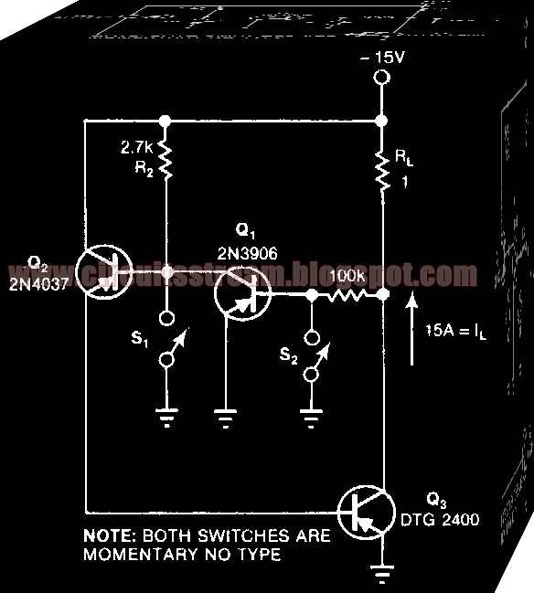

 simple scr replacing latching switch circuit diagram

 The current, !1, to be switched is 15 A. Momentarily depressing S2 removes Ql`s base drive, turning Ql off and allowing Q2 to tum on. Q2 then drives the base-emitter junction of Q3, turning Q3 on. Q3`s collector-emitter voltage, which ·serves as Ql`s base drive, is essentially zero, keeping Ql off. To tum Q3 off, depress Sl; this action momentarily shunts Q2`s base current to ground, reversing the chain of events that turned Q3 on.
Read More..

Monday, September 1, 2014

Simple Ni cad charger Wiring diagram Schematic

Simple Ni-cad charger Circuit Diagram uses constant current LEDs to adjust charging current. It makes use of LEDs that pass a constant current of about 15 mA for an applied voltage range of 2-18 V. They can be paralleled to give any multiple of 15 mA and they light up when current is flowing.The schema will charge a single cell at 15, 30 or 45 mA or cells in. series up to the rated supply voltage limit (about 14 V).

 Simple Ni-cad charger Circuit Diagram

Simple
 
Read More..

Sunday, August 31, 2014

Simple FM transmitter circuit 88 108MHz


This is simple transmitter schema diagram.This schema has some what good coverage.To tune this schema use 88MHz-108MHz radio.This schema can be operated with 9-12V power supply.This schema needs 30mA.


Note

#In some countries transmitters have been banned.so dont misuse this schema.We just wanted to give you an extra knowledge about it.If somebody used this for unnecessary things we cant get the responsibility of it.
Read More..

Saturday, August 30, 2014

Simple Light Sensor Alarm circuit with NE555

This schema sent out an alarm when its LDR sensor is exposed to light by sun or lamp. A 555 astable multivibrator was used here which sent signal a tone of about 1kHz upon detecting light.The sensor when exposed by light completes the schema and makes the 555 oscillate at about 1kHz with transistor to drive current.

The sensor is also shown in the schema diagram. It has to placed making an angle of about 30 – 45 degrees to the ground.

Sensitivity can be adjust with P1.  This makes the sun light to flow through it to the ground and prevents the alarm from going on due to the stored light on the sensor.

Simple

Read More..

Friday, August 29, 2014

Simple Voice Switch on Wiring diagram Schematic

This is a simple voice activated or switch on schema diagram. With this sound activated switch, control by sound may be very useful, not just on a robot but also for a bit of home automation.This schema provides either latched switching or timed switching. U1A and UlB provide audio amplification from the microphone. U2 is a retriggerable monostable multivibrator. 

 Simple Voice Switch on Circuit Diagram


Simple

SI A and SIB select either U3, a flip-flop, or U2. R13 and R14 allow a 6- to 60-second timer delay after the sound ceases, in the timed mode. BR1, U5, and associated components form a power supply. Ql drives opto coupler U4 and triggers triac TRl. -If desired, four silicon diode rectifiers connected as a bridge can be substituted for BR1. Just make certain the diodes are rated at least 50V, 1A.
Read More..

Thursday, August 28, 2014

Simple Temperature Sensing Diodes Selector Circuit Diagam

Low-cost semiconductor diodes such as 1N914, 1N4148 and 1N400X can be used as temperature sensors in applications where high accuracy is not required. They can be mounted on transistors, power diodes, transformers, heat sinks, rechargeable batteries, crystals, PCB, etc to monitor their temperature.

It is highly desirable to use temperature sensors with linear temperature characteristics and the mentioned diodes are best suited for that. To use them as temperature sensors, these diodes first need to be sorted according to their temperature coefficient. (Please refer ‘Signal Diode-Based Fire Alarm’ schema idea published in February 2013 issue to understand how these diodes can be used as temperature sensors.) This schema can help quickly sort different diodes based on their temperature coefficient.

Circuit and working
The schema diagram of the device for selection of temperature-sensing diodes is shown in Fig. 1. The schema is built around step-down transformer X1, voltage regulator 7818 (IC1), voltage regulator 7809 (IC2) and three diodes 1N4001 (D1 through D3). The mains supply is stepped down to 21V, 250mA using transformer X1. Diode D2 is sufficient to rectify it since the required output current is typically below 20mA. The linear regulator IC1 provides the 18V power supply for the diodes (connected at CON1 through CON12) to be tested. The linear regulator IC2 provides the 9V power supply for the digital voltmeter (DVM) used for measuring the voltage drop across diodes.

Simple
Fig. 1: Circuit diagram of the device

Fig. 2: An actual-size, single-side PCB for device for selecting diodes


Fig. 3: Component layout of the PCB

Utilising this device, it is possible to test the diodes at around 0.1mA of forward current. The current for their PN junctions is provided through individual resistors R1 through R12. The value of a resistor is much higher that the resistance of the tested diode’s junctions, so changing the diodes will not change the forward current significantly.

 
The number of the connectors for the test diodes can be increased or decreased. The device does not need any adjustment or calibration to operate properly. To calculate the temperature co-efficient (TKU) of each diode and to sort the diodes accordingly, we need to measure the voltage drop across the diodes under test.

To sort the diodes, ensure that all of them are connected in the schema and the voltage drop (say U1) across each diode is measured one by one at the same temperature, say 25°C. The voltages can be read at TP3 through TP14 with respect to TP0 using the DVM as shown in Fig. 1. Now change the temperature to, say, 40°C, and take the measurements (say U2) again. We can use an electrical equipment, such as a heater, to produce the second temperature. So now the temperature coefficient of the PN junction for a diode will be:

TKU = (U1-U2)/(T1-T2), mV/°C

The voltage drop change of the PN junction due to temperature change is linear, so we should take measurements at only two temperatures for each diode. The test temperatures can be the same for all the diodes or different. Most of the diodes can be used in the temperature range of -25°C to +150°C without any problem. The temperature coefficient of most of the PN junctions is in the range of -1.3mV/°C to -3mV/°C, so we can use these diodes as sensors.

Construction and testing
An actual-size, single-side PCB for the device is shown in Fig. 2 and its component layout in Fig. 3. After assembling the schema on PCB, enclose it in a suitable plastic case.

To test the schema for proper functioning, verify correct power supply for the diodes and DVM at TP1 and TP2 with respect to TP0. Voltage drop across each diode can be verified at TP3 through TP14. 


Sourced By: EFY : Author: Petre Tzv. Petrov
Read More..

Simple Universal Laboratory Power Supply Wiring diagram Schematic

This is the Simple Universal Laboratory Power Supply Circuit Diagram. The value of the design lies in the use of IC1, an LM317HVK adjustable s.eries-pass voltage regulator, for broad-range performance remainder supplies voltage-setting and current-limiting functions. 

The input to ICI-comes from the output of BR1, which is filtered by CI and C2 to about +60 Vdc, and the input for current-sense comparator IC2 comes from BR2, which also acts as a negative bias supply for regulation down to ground.

Universal Laboratory Power Supply Circuit Diagram

Universal


Simple Universal Laboratory Power Supply Circuit Diagram
Read More..

Tuesday, August 26, 2014

Simple Variable Dc Supply Step Wiring diagram Schematic

This is a Simple Variable Dc Supply Step Circuit Diagram. Intended as a replacement for generally poorly regulated `wall-type` ac/dc adapters, this Simple Variable Dc Supply Step Circuit Diagram offers superior performance to simple, unregulated adapters. 

Voltages of 3, 6, 9, and 12 V are available. The DPDT switch serves as a polarity-reversal switch. R2 through R6 can be replaced with a 2.5-kfl pot for a variable voltage of 1 to 12 V. R7 through RIO can be replaced by a fixed resistor of about 1 kfi if the LED1 brightness variation with output voltage is not a problem.

Simple Variable Dc Supply Step Circuit Diagram

Simple

Read More..

Monday, August 25, 2014

Versatile and simple power supply

Versatile and simple power supply is one of several series of power supply many other well-known, because making a fairly easy circuit power supply is also nice, versatile addition also can be used on any circuit, for example, Radio tuner, Intregated power amplifier circuit, etc. . But we need to know the Versatile and simple power supply is not used to charge the battery because it will quickly damage the transistors that exist. To have a good output voltage, use of quality components.
Versatile
Versatile and simple power supply
Part List :
R1 = 1K
C1 = 0.22uF 275V
C2 = 4700uF 50V
C3 = 100n
C4 = 220uF
C5 = 1000uF
Q1 = TIP30
T1 = Step-down Transformer 220V to 12-35V
Read More..

Saturday, August 23, 2014

Mini and simple power amplifier circuits

low

What is the meaning of the picture above? The above picture is a miniature audio amplifier and very simple. Here I will give an audio amplifier schematic is very simple which only requires a few components only, can be seen under this scheme.
Read more
Read More..

Friday, August 22, 2014

Simple LM358 Mic Preamplifier

Simple


This is a simple LM358 microphone preamplifier schematic diagram. The pre-amp schema is very easy to build and.. its a low cost project... The variable resistor R5 is to adjust the LM358 op-amp gain. The LM358 has dual op-amp schema modules, you may use a single LM358 to build two channels mic preamplifier.

Parts List:
R1, R3, R4 = 10K
R2 = 1K
R5 = 100K-1M Potensiometer
C1 = 0.1uF
C2 = 4.7uF/16V
IC1 = LM358 dual op-amp single power supply
Mic = Electret Microphone
Read More..