Showing posts with label with. Show all posts
Showing posts with label with. Show all posts
Thursday, November 20, 2014
Interface Relay with PNP transistor
One technique relay drivers from the microcontroller or computer can be made with the driver PNP transistors like the article "Interface Relays With PNP Transistor" ini.This circuit interface is simple and easily applied to a microcontroller or computer parallel port. Interface Relays With PNP Transistor uses 2 transistors 2N3904 and 2n2905/2N2907 UAH as a power relay drivers. The advantages of this circuit can menggeran relay with considerable power with TTL logic input from the computer and microcontroller. Source voltage required to follow the relay circuit is used, for example using a 12V relay, the source voltage to 12V or 24V relays the 24V voltage source. Detailed relay interface circuit and microcontroller or computer can be seen in the following figure.

Function diodes mounted parallel with the relay to prevent backflow into the transistor due to magnetic induction of the relay coil, therefore these diodes must be installed. For installation with a microcontroller or computer which need to be noticed is the Grund computer or microcontroller circuit must be connected to ground in series Interface Relays With this PNP transistors.

Wednesday, November 19, 2014
Simple Power Supply with 2 transistors
Power Supply in this post is using a regulator which is composed of 2 pieces of NPN transistor. A transistor acts as a power regulator and a transistor again serves as a controller output voltage. Power Supply has an adjustable output with a range of 6-12 VDC. The part that serves as a power regulator is Q1 TIP31. Then the controller output voltage is a voltage divider composed of R3, R4, VR1 and R2 provide bias to the base of Q2 to control the power regulator Q1. In a series of power supply is mounted 5.1 V zener diode which serves to make the minimum limit the output voltage with Q2.
Power Supply With transistor circuit is quite simple and can be made with the PCB holes, so for those who want to try to directly mempraktikannya. May the power supply circuit can be useful for readers, especially for friends who need a power supply circuit with the regulator transistor.
Tuesday, November 18, 2014
Running LED with 4017
Running LED with 4017 complete with PCB layout. The series of 8 LED current is the basis for creating an 8-point LED. Slightly different from the running LED with IC 4017 (decade counter), 8 running this led is lit in sequence, but that has been previously flame does not die when the led is lit afterwards. 8 led to death after led to the fire-8. Meanwhile in the running LED (decade counter), the system LED lights like "point", there is only one LED that flashes between the tenth led.
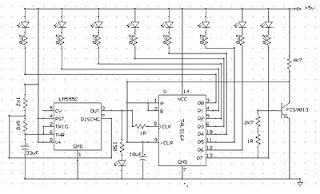
The main component is the IC 74LS164 (SHIFT REGISTER), with its timer is astable multivibrator circuit (using IC NE555).
The series will be more efficient when using a stable power supply (regulator) using IC Regulator 7805. Under this scheme a series of stable power supply 5 volts dc.

Monday, November 3, 2014
Power Amplifier with 2N3055
Simple and low cost. The optimal supply voltage is around 50V, but this amp work from 30 to 60V. The maximal input voltage is around 0.8 – 1V. As you can see, in this design the components have a big tolerance, so you can build it almost of the components, which you find at home. The and transistors can be any NPN type power transistor, but do not use Darlington types… The output power is around 60W.
Some comments:
- capacitor C1 regulates the low frequencies (bass), as the capacitance grows, the low frequncies are getting louder.
– capacitor C2 regulates the higher frequencies (treble), as the capacitance grows, the higher frequencies are getting quiter. – this is a class B amplifier, this means, that a current must flow through the end transistors, even if there is no signal on the input. This current can be regulated with the 500? trimmer resistor. As this current incrases, the sound of the amplifier gets better, but the end transistors are more heating. But if this current decrases, the transistors are not heating so much, but the sound gets worse…
Read More..
Some comments:
- capacitor C1 regulates the low frequencies (bass), as the capacitance grows, the low frequncies are getting louder.
– capacitor C2 regulates the higher frequencies (treble), as the capacitance grows, the higher frequencies are getting quiter.
 – this is a class B amplifier, this means, that a current must flow through the end transistors, even if there is no signal on the input. This current can be regulated with the 500? trimmer resistor. As this current incrases, the sound of the amplifier gets better, but the end transistors are more heating. But if this current decrases, the transistors are not heating so much, but the sound gets worse…
 Friday, October 31, 2014
Operational Amplifiers with Power Supply
The single feed mode has become very important in systems powered from a single power supply, because it reduces the cost of circuits with operational amplifiers and also makes it easier to use on mobile devices. In this series of articles will look at various ways that can power amplifiers circuits using operational amplifiers with single power supply (single rail).
The diagram of a sound amplifier, which operates with a single power supply shown in Figure 16. In this circuit one end of the signal source connected to the right input terminal of the operational amplifier, and the other end connected to the bias voltage VBias.
The load resistance (RL) and R1 also associated with the bias voltage. The voltage at the right input terminal, VP, is equal to:
The voltage at the reverse input terminal VN, is equal to:
The diagram of a sound amplifier, which operates with a single power supply shown in Figure 16. In this circuit one end of the signal source connected to the right input terminal of the operational amplifier, and the other end connected to the bias voltage VBias.
The load resistance (RL) and R1 also associated with the bias voltage. The voltage at the right input terminal, VP, is equal to:
Vp = VBias + Vin
The voltage at the reverse input terminal VN, is equal to:
VN = VD + VP but because,
Vd = 0 we have:
VN = VP = Vin + VBias
without an input signal
Vin = 0, so therefore
Vn = Vp = VBias
Vd = 0 we have:
VN = VP = Vin + VBias
without an input signal
Vin = 0, so therefore
Vn = Vp = VBias
Figure 16. Amplifier with single power supply.
Figure 17. Input and output waveforms of the amplifier of Figure 16.
The bias voltage (VBias) is typically equal to half the voltage of the power supply. The output voltage of this amplifier can be calculated as follows:
The current I1, which flows through the resistor R1, is approximately equal to the current I2, which flows through the resistor R2, and thus I1 = I2. The current flowing through R1 is equal to the difference voltage across R1 divided by the value of R1, ie

In this circuit VB is the voltage applied to the right end of R1, and VA is the voltage applied to the left end of R1.
From the figure 16 we see that:
VB = VP but VP = VBias + VIN, thus:
VB = VBias + VIN
We also have VA = VBias so:

Similarly, the current I2 flowing through the resistor R2, is equal to the difference voltage across the R2.
i.e. VR2 = VO - VB divided by the value of R2
We also have VB = VBias + VIN, thus:

Figure 18a. AC amplifier with simple power supply.
Since I1 = I2, we obtain:

Rearranging we get:


So in the absence of an input signal, ie when VIN = 0, the above equation becomes

or VO = VBias
So in the absence of an input signal, the input terminals and the output terminal of the operational amplifier have the same voltage (VBias).
If an input voltage 2 volts peak to peak, is applied to the amplifier shown in Figure 16, R1 = R2, and VCC = 10V, then when the input signal is at the positive peak value of +1V, the output voltage will be:


When the input signal changes is at its highest negative value -1V, then the output voltage equals:

So when the input signal changes from -1V to +1V, the output voltage varies from +3V to +7V.
Figure 17 shows waveforms of the input and output. Notice that the first term in equation 1 represents the voltage gain of a conventional amplifier using a double power supply. The voltage gain is given by the following relationship:

In a conventional non-inverting amplifier, which operates with double supply, the bias voltage VBias is equal to 0 volts, and the output voltage is given by the following equation:

Monday, October 27, 2014
Subwoofer Filter with LM741
The acoustics of converting a filter, near are many aspects of the financially viable possibility of the further famous are Baxandal filter low and soaring frequency filters and crossover Acoustic area is transformed into subordinate-domains, so with the purpose of the Thursday Speakers. Applications, we offer a filter, the limits of the region to transform acoustic (20-20000Hz) happening the region of 20-100Hz.

Read More..

The make signs on behalf of a head high pass filter C1, C2, P1, which is undesirable level DC input. A lowpass filter consisting of R3, R4, C3 prevents frequencies on top of 10 kHz, which look after not benefit from this design, and it would come about so as to the instability and clatter. The precipitate amp invert make signs.
The low Summary of the amplifier signals extend to a next low-pass filter to prevent the frequency from the speakers.
I unambiguous, a second order, because this box with a bunged place bring out. If you give birth to a circuit with a valve coordination, and therefore simply close the Wind (Roll a pair off of socks and pick by the docks / Wind), this preference bequeath you a sealed box as a replacement for.
Friday, October 24, 2014
FM Radio Receiver Circuit with IC TDA 7012T
FM Radio Receiver IC TDA 7012T is very simple, but it has an FM radio receiver sensitivity and good selectivity. Single Chip FM Receifer cool name of IC TDA7012T 7012T TDA is to build an FM receiver requires a few additional components.
Feature contained in FM receiver IC TDA 7012T is quite tempting to an FM receiver. Among features an FM receiver TDA 7012T is a low-voltage applications micro affability arrangement (MTS), Frequency Loked Loop (FLL) to 76 KHz range and selectivity of FM receiver with RC Filter. In an article by FM Radio Receiver IC TDA 7012T can be seen in the FM receiver circuit which can be made.


FM Radio Receiver with IC TDA 7012T
From the picture above components to make the FM Radio Receiver IC TDA 7012T as follows:
R1 = 8kΩ2
R2 = 10kΩ
R3 = 390Ω
C1, C3 = 10nF
C2, C6, C9, C16 = 100nF
C4 = 33pF
C5 = 25pF trimmer
C7, C10 = 1nF5
C8 = 820pF C11 = 1NF
C12 = 68pF
C13 = 220pF
C14 = 47μF 10V
C15 = 3nF3
L1 = 36nH
L2 = 1μH,
IC1 = TDA7021T
Thursday, October 23, 2014
Mini Amplifier with 3 Transistor
Mini 3 transistor amplifier is a simple amplifier with 50mW power drawn by 3 transitor.
The series of three mini-amplifier transistors can be used for loud speaker 8 ohm load. Source voltage required to activate the mini-amplifier can be drawn from the batteries 9V.Rangkaian 3 transistor amplifier is often used in simple portabe audio devices such as radios or small tape recorder. Mini-transistor amplifier circuit 3 is quite simple as shown in the figure below.

Mini-transistor amplifier circuit 3 includes type of amplifier OTL (Output Transformer Less). Mini-transistor amplifier circuit 3 is used for output coupling capacitors. Amplifier circuit is simple and suitable when used for audio amplifier experiment.
Read More..
The series of three mini-amplifier transistors can be used for loud speaker 8 ohm load. Source voltage required to activate the mini-amplifier can be drawn from the batteries 9V.Rangkaian 3 transistor amplifier is often used in simple portabe audio devices such as radios or small tape recorder. Mini-transistor amplifier circuit 3 is quite simple as shown in the figure below.
Mini-transistor amplifier circuit 3 includes type of amplifier OTL (Output Transformer Less). Mini-transistor amplifier circuit 3 is used for output coupling capacitors. Amplifier circuit is simple and suitable when used for audio amplifier experiment.
Thursday, September 18, 2014
10W AUDIO AMPLIFIER WITH MUTING
DESCRIPTION
The TDA 1910 is a monolithic integrated circuit in MULTIWATT® package, intended for use in Hi-Fi audio power applications, as high quality TV sets. The TDA 1910 meets the DIN 45500 (d = 0.5%) guaranteed output power of 10W when used at 24V/4W. At 24V/8W the output power is 7W min.
Features:
- muting facility
- protection against chip over temperature
- very low noise
- high supply voltage rejection
- low "switch-on" noise.
- easy assembly
- simple heatsink
Circuit Diagram
 |
| 10W AUDIO AMPLIFIER WITH MUTING |
Tuesday, September 9, 2014
Simple 10 000x With One Transistor
For a collector follower with emitter resistor, you’ll often find that the gain per stage is no more than 10 to 50 times. The gain increases when the emitter resistor is omitted. Unfortunately, the distortion also increases. With a ubiquitous transistor such as the BC547B, the gain of the transistor is roughly equal to 40 times the collector current (Ic), provided the collector current is less than a few milliamps. This value is in theory equal to the expression q/KT, where q is the charge of the electron, K is Boltzmann’s constant and T is the temperature in Kelvin.
For simplicity, and assuming room temperature, we round this value to 40. For a single stage amplifier schema with grounded emitter it holds that the gain Uout /Uin (for AC voltage) is in theory equal to SRc. As we observed before, the slope S is about 40Ic. From this follows that the gain is approximately equal to 40I cRc. What does this mean? In the first instance this leads to a very practical rule of thumb: that gain of a grounded emitter schema amounts to 40·I c·Rc, which is equal to 40 times the voltage across the collector resistor.
If Ub is, for example, equal to 12 V and the collector is set to 5V, then we know, irrespective of the values of the resistors that the gain will be about 40R(12–5) = 280. Notable is the fact that in this way the gain can be very high in theory, by selecting a high power supply voltage. Such a voltage could be obtained from an isolating transformer from the mains. An isolating transformer can be made by connecting the secondaries of two transformers together, which results in a galvanically isolated mains voltage.
For simplicity, and assuming room temperature, we round this value to 40. For a single stage amplifier schema with grounded emitter it holds that the gain Uout /Uin (for AC voltage) is in theory equal to SRc. As we observed before, the slope S is about 40Ic. From this follows that the gain is approximately equal to 40I cRc. What does this mean? In the first instance this leads to a very practical rule of thumb: that gain of a grounded emitter schema amounts to 40·I c·Rc, which is equal to 40 times the voltage across the collector resistor.
If Ub is, for example, equal to 12 V and the collector is set to 5V, then we know, irrespective of the values of the resistors that the gain will be about 40R(12–5) = 280. Notable is the fact that in this way the gain can be very high in theory, by selecting a high power supply voltage. Such a voltage could be obtained from an isolating transformer from the mains. An isolating transformer can be made by connecting the secondaries of two transformers together, which results in a galvanically isolated mains voltage.
Circuit diagram:

10,000x With One Transistor Circuit diagram
That means, that with a mains voltage of 240 Veff there will be about 340 V DC after rectification and filtering. If in the amplifier schema the power supply voltage is now 340 V and the collector voltage is 2 V, then the gain is in theory equal to 40 x (340–2). This is more than 13,500 times! However, there are a few drawbacks in practice. This is related to the output characteristic of the transistor. In practice, it turns out that the transistor does actually have an output resistor between collector and emitter.
This output resistance exists as a transistor parameter and is called ‘hoe’. In normal designs this parameter is of no consequence because it has no noticeable effect if the collector resistor is not large. When powering the amplifier from 340 V and setting the collector current to 1 mA, the collector resistor will have a value of 338 k. Whether the ‘hoe’-parameter has any influence depends in the type of transistor. We also note that with such high gains, the base-collector capacitance in particular will start to play a role.
As a consequence the input frequency may not be too high. For a higher bandwidth we will have to use a transistor with small Cbc, such as a BF494 or perhaps even an SHF transistor such as a BFR91A. We will have to adjust the value of the base resistor to the new hfe. The author has carried out measurements with a BC547B at a power supply voltage of 30 V. A value of 2 V was chosen for the collector voltage. Measurements confirm the rule of thumb. The gain was more than 1,000 times and the effects of ‘hoe’ and the base-collector capacitance were not noticeable because of the now much smaller collector resistor. Link
Sunday, September 7, 2014
Simple Comparator with time out Wiring diagram Schematic
This is a Simple Comparator with time out Circuit Diagram. The MC1422 is used as a comparator with input (Pin 5). The frequency of the pulses for the capability of a timing output pulse when the the values of R2 and Cl as shown is approx i-inverting input (Pin 6) is the non inverting mately 2 Hz, and the pulse width 0 ms.
Simple Comparator with time out Circuit Diagram
Friday, September 5, 2014
300W Power Amplifier Circuit with 2N773
Power Amplifier 300W with transistor 2N3773
This amplifier was designed to provide a use for the otherwise useless TO3 power transistors that many hobbyists have in their junk pile. With good construction the module is capable of high quality performance and is rated to 300 watts into a 4 ohm load depending on power supply. With the driver and output transistors specified it is limited to DC rails of +/- 70 volts.
| Power Amplifier Circuit Diagram |
5W 5W AMPLIFIER WITH DC VOLUME CONTROL TDA7496
Circuit Diagram:
 |
| 5W+5W AMPLIFIER WITH DC VOLUME CONTROL |
Wednesday, September 3, 2014
Power amplifier 65W with HEXFET
A medium power amplifier that is characterized by a lot of good sound quality, but simultaneously is very simple in the construction. full article here

Tuesday, September 2, 2014
Universal Power Supply Circuit with IC LM317
This circuit is universal power supply , you can use this circuit to supply . On the IC you can adjustable regulator provides short circuit protection and automatic voltage adjust . The input voltage to the circuit regulator is supplyed by AC 220 V / 110 V and down voltage by transformator then rectified by bridge diode . And output voltage is clear and stabilized .

Wiring a second LM317 , U2 , in parallel with U1 is a quick and clean way to increase the current limiting threshold to 3A without sacrifing short-circuit protection.When more than 3A is required , the regulator module can be used to drive the base of one or more pass-transisotrs.
DC motor driver with H Bridge IC L293D
Making a DC motor driver with H-Bridge technique can use IC L293D as in the article "DC Motor Driver H-Bridge L293 (2 Motor DC)"is. DC motor driver L293D can be used to control the DC motor 2 pieces at once. DC Motor Driver L293D can be used to control a DC motor continuously or with a PWM technique. Dc motor driver circuit in the article "DC Motor Driver H-Bridge L293 (2 Motor DC)" only use IC L293D only. For more details see the following figure.
Working system of DC motor driver L293D is to provide control signals in the form of logic or pulse to the input lines 1A - 1B for DC motor control M1 and the input 2A - 2B for the control of DC motor M2 with the following conditions:
Input A Input B Motor DC0 0 Motor silent
1 0 motor rotates counterclockwise
0 1 Motor berputer clockwise
1 1 Motor silent
Description: Enable Input given a logic 1 to obtain such data in the table above.
Saturday, August 30, 2014
Simple Light Sensor Alarm circuit with NE555
This schema sent out an alarm when its LDR sensor is exposed to light by sun or lamp. A 555 astable multivibrator was used here which sent signal a tone of about 1kHz upon detecting light.The sensor when exposed by light completes the schema and makes the 555 oscillate at about 1kHz with transistor to drive current.
The sensor is also shown in the schema diagram. It has to placed making an angle of about 30 – 45 degrees to the ground.
Sensitivity can be adjust with P1. This makes the sun light to flow through it to the ground and prevents the alarm from going on due to the stored light on the sensor.
Friday, August 29, 2014
Schematic Audio Power Amplifier with IC AN7118S
*notif : this circuit is stereo power amplifier
Although the schematic power amplifier with IC AN7118S is difficult for lees understood making of PCB track . But once tried to design on PCB is not so difficult. Because the actual components close together and easy to design it. This Circuit need minimum voltage 1 volt and maximum voltage 3 volt. It is a low voltage amplifier with power output 2 x 35 m Watt .
Schematic circuit below :
 | ||
| Click to Enlarge |
Components Required :
Resistor / Condensator / Capacitor : 4,7Ohm (2x) , 0,01 uF (2x) , 47uf (2x) , 68 pf (2x) , 1uF (2x) , 22uF (2x) , 220 uF (1x) , 470uf (2x). Condensator / capacitor voltage use 16 volt. Only Condensator on output speaker use voltage 25 volt.
Tuesday, August 26, 2014
FM Radio Receiver Circuit with IC TDA 7012T
TDA 7012T FM Radio Receiver
FM Radio Receiver IC TDA 7012T is very simple, but it has an FM radio receiver sensitivity and good selectivity. Single Chip FM Receifer cool name of IC TDA7012T 7012T TDA is to build an FM receiver requires a few additional components.
Feature contained in FM receiver IC TDA 7012T is quite tempting to an FM receiver. Among features an FM receiver TDA 7012T is a low-voltage applications micro affability arrangement (MTS), Frequency Loked Loop (FLL) to 76 KHz range and selectivity of FM receiver with RC Filter. In an article by FM Radio Receiver IC TDA 7012T can be seen in the FM receiver circuit which can be made.FM Radio Receiver with IC TDA 7012T
From the picture above components to make the FM Radio Receiver IC TDA 7012T as follows:
R1 = 8kΩ2
R2 = 10kΩ
R3 = 390Ω
C1, C3 = 10nF
C2, C6, C9, C16 = 100nF
C4 = 33pF
C5 = 25pF trimmer
C7, C10 = 1nF5
C8 = 820pF C11 = 1NF
C12 = 68pF
C13 = 220pF
C14 = 47μF 10V
C15 = 3nF3
L1 = 36nH
L2 = 1μH,
IC1 = TDA7021T
Hopefully useful and become an idea in the manufacture of Mini FM Receiver with IC TDA 7012T
Tuesday, August 19, 2014
10 10 W Stereo Amplifier with Tda 2004
Hello! in this post I will show a small amplifier using integrated schema TDA2004 get two outputs 10 watts, the schema is very simple, if you want to change the schema, or a mono version refer to the datasheet tda2004!
The schema is powered by source between 12 and 15 volts with a current of 1.5 Amperes.
The schema is powered by source between 12 and 15 volts with a current of 1.5 Amperes.
See the figure below:
Subscribe to:
Posts (Atom)
