Showing posts with label circuit. Show all posts

Monday, January 26, 2015

Aviation Intercom Circuit

Before its move offshore, I was lucky enough to be involved in developing the avionics system for the Flightship Ground Effect FS8 craft (see www.pacificseaflight.com/craft.shtml). Although officially classed as a boat, it has wings and can travel at 180km/h some three metres above the water. The communications system was adapted from an aircraft unit and was a particular problem. It was expected to allow speech between the two pilots and radio, as well as receive audible warnings from the onboard computers and feed sound to the onboard data logger. Initially, the system was very noisy due to ground loops and incompatibility problems.

A circuit similar to that shown here was the solution. Although optimised to suit Softcom brand headphones with active noise reduction, it should be suitable for most aviation sets. The plugs indicated are standard aviation types but are insulated from the instrument panel to eliminate earth loops. The inputs from the two pilots microphones are summed and amplified by transistors Q1 & Q2. When one pilot presses his or her transmit key (mounted on the yoke), the transmit relay (RLY1) closes, muting the other pilot’s microphone via the optocoupler (OPTO1).

Aviation Intercom Circuit Diagram:

intercom-circuit-diagram

The outputs from the microphone preamp, computer audio transformer (T1) and radio speaker transformer (T2) are summed via 10kΩ resistors and applied to the input of IC1, an LM386 audio amplifier. Note that transformers are used here to avoid creating additional earth loops. The output of the LM386 drives the pilots’ headphones via transformers T3 & T4, which are needed for impedance matching. Each audio source has its own level control (VR1, VR3 & VR4). The main volume control (VR5) is included to allow for ambient noise level. VR2 is used to set the signal level for the data logger.
 
Read More..

Friday, December 12, 2014

Solar Battery Charger Circuit Schematic

solar-charger

Here is a solar charger circuit that is used to charge Lead Acid or Ni-Cd batteries using the solar energy power. The circuit harvests solar energy to charge a 6 volt 4.5 Ah rechargeable battery for various applications. The charger has Voltage and Current regulation and Over voltage cut off facilities. 
Read More..

Mini Subwoofer Circuit 22W

audio-schematic-diagram

The subwoofer is a subwoofer or a speaker to reproduce low frequencies, devotee of 20 Hz to 150 Hz electronic circuit diagram below shows the details of a scheme of the main amplifier TDA1516 22 watt in 4 ohm car subwoofer driver. This device is designed for an existing stereo amplifier, often requires adding another blow to the music of driving a subwoofer.
Read More..

Thursday, November 20, 2014

A 4 Digit Keypad Controller Switch Circuit

A 4-Digit Keypad Controller Switch Circuit

This is a universal version of the Four-Digit Alarm Keypad . I have modified the design to free up the relay contacts. This allows the circuit to operate as a general-purpose switch. It also means that it can be used to control all of my Alarm Circuits. Ive used a SPCO/SPDT relay - but you can use a multi-pole relay if you wish.

The relay is energized by pressing a single key. Choose the key you want to use - and connect it to terminal "E". Choose the four keys you want to use to de-energize the relay - and connect them to "A B C & D". Wire the common to R1 and all the remaining keys to "F".

The Circuit is easy to use. When you press "E" - current through D2 & R9 turns Q6 on - and energizes the relay. The two transistors - Q5 & Q6 - form a "Complementary Latch". So - when you release the key - the relay will remain energized.

To de-energize the relay - you need to press keys "A B C & D" in the right order. When you do so - pin 10 of the IC goes high - and it turns Q4 on through R8. Q4 connects the base of Q6 to ground. This unlatches the complementary pair - and the relay drops out.

Any keys not wired to "A B C D & E" are connected to the base of Q3 by R7. Whenever one of these "Wrong" keys is pressed - Q3 takes pin 1 low and the code entry sequence fails. If "C" or "D" is pressed out of sequence - Q1 or Q2 will also take pin 1 low - with the same result. If you make a mistake while entering the code - simply start again.

The Keypad must be the kind with a common terminal and a separate connection for each key. On a 12-key pad, look for 13 terminals. The matrix type with 7 or 8 terminals will NOT do. With a 12-key pad - over 10 000 different codes are available. If you need a more secure code - use a bigger keypad with more "Wrong" keys wired to "F". A 16-key pad gives over 40 000 different codes.
Read More..

RS232 to RS485 Circuit

The new archetypal of RS485 advocate overcomes the RTS controlled botheration accomplished by our chargeless design. However, to do that requires a microprocessor, so there is a greater complication to the design. We advertise this unit, although currently we are attached our sales to barter who can pay by coffer alteration – which in absoluteness is bounded Australian companies. 

This architecture has been almost agitation free, and if you crave quantities we can acclimate the adapter pinout to clothing your appliance – about again the accessory will no best fit the simple little D25 case in which you see it pictured.

  RS232 to RS485 Circuit

* Data (vs RTS) controlled – does not rely on PC handshake timing
* DB25 RS232 connector compatible with PC
* TxD and RxD translated from RS232 to RS485
* Direction of transmission controlled by Data
* Handshake loop the PC connection so it works with all software
* RS485 signals output on D9 male with lots of Ground pins
* Indicator LED(s) to show communications traffic
* Line powered – powered by RS232 handshake lines
* RS485 Termination resistor not included
* Pullup/Pulldown resistors on RS485 to establish line-idle condition
* Baud rate is dipswitch selectable 1200 – 115.2k
Read More..

Monday, November 17, 2014

Preamplifier Circuit Diagram DCF77

DCF77 Preamplifier Circuit Diagram A popular project among microcontroller aficionados is to build a radio-controlled clock. Tiny receiver boards are available, with a pre-adjusted ferrite antenna, that receive and demodulate the DCF77 time signal broadcast from Mainf lingen in Germany.
DCF77 has a range of about 1,000 miles. All the microcontroller need do is decode the signal and output the results on a display. The reception quality achieved by these ready-made boards tends to be proportional to their price. In areas of marginal reception a higher quality receiver is needed, and a small selective preamplifier stage will usually improve the situation further. 

The original ferrite antenna is desoldered from the receiver module and connected to the input of the preamplifier. This input consists of a source follower (T1) which has very little damping effect on the resonant circuit. A bipolar transistor (T2) provides a gain of around 5 dB. The output signal is coupled to the antenna input of the DCF77 module via a transformer

Circuit diagram: 
DCF77 Preamplifier Circuit Diagram

DCF77 Preamplifier Circuit Diagram The secondary of the transformer, in conjunction with capacitors C4 and C5, forms a resonant circuit which must be adjusted so that it is centered on the carrier frequency. An oscilloscope is needed for this adjustment, and a signal generator, set to generate a 77.5 kHz sine wave, is also very useful. This signal is fed, at an amplitude of a few milli-volts, into the antenna input. With the oscilloscope connected across C4 and C5 to monitor the signal on the output resonant circuit, trimmer C5 is adjusted until maximum amplitude is observed.

It is essential that the transformer used is suitable for constructing a resonant circuit at the carrier frequency. Our proto-type used a FT50-77 core from Amidon on which we made two 57-turn windings. It is also possible to trim the resonant frequency of the circuit by using a transformer whose core can be adjusted in and out. In this case, of course, the trimmer capacitor can be dispensed with. Rainer Reusch Elektor Electronics 2008
Read More..

Atmel microcontroller Easy Downloader Circuit

Easy Downloader Circuit
Atmel microcontroller series AT89Cxx51 Easy Downloader is one of the downloader that is often used to write data to program the Atmel microcontroller AT89CXX51. Easy Downloader AT89Cxx51 ATMEL microcontroller is using the serial port as a channel of communication with the computer. 


Easy Downloader ATMEL Microcontroller AT89Cxx51 can be used to program Atmel AT89CXX51 in parallel. Atmel microcontroller series AT89Cxx51 Easy Downloader is quite simple to make your own because the components necessary to membutanya not complex. Atmel microcontroller series AT89Cxx51 Easy Downloader do not support the serial programming microcontrollers ISP. In the article Easy Downloader ATMEL Microcontroller AT89Cxx51 only displays images Easy Downloader Microcontroller series from Atmel AT89Cxx51 only and are simple.
Read More..

Sunday, November 16, 2014

Tone control low noise circuit

Tone control or pre-amplifier is an amplifier circuit supporters. Sometimes some of us do not know where a good amplifier, a raft alone and the results are not much different or even the same. Therefore we must know the character of the advantages and disadvantages of each amplifier equipment.

Tone control low noise here does not mean without noise, but noise compared with the lowest tone control on the market, for example Ronica transistor 4, TL-084, TC-2 LM833 etc.

CSE | Circuit Schematic Electronics

Jump toexplanation of each component ...

Potensio 1 serves to regulate the intensity / level of the incoming signal is assisted potensio 2 as balance / counterbalance. Potensio 2 is still installed and is usually an optional component. 1-2uF/250V capacitor R1 is actually a brand name,but I prefer to replace it with a 1K resistor / 5% normal for reasons to avoid hum and interference sensitive. R2 R3 while minimizing interruption to adjust the impedance OP-amp 1. R4 and R5 serves to increase the gain of 1.3 times. Pre amplifiers typically use a strengthening standards by 2 times, but by most of us think it has a noise. So I chose the value of 1.3 times, but the most minimal noise signal from the volume is enough to make the lamp light peak.

For low noise ...Cause of noise in op amp 1, apex audio even eliminate this stage. CanThis step is also used as a buffer (jumper R5), the strengthening of a time. Lower values ​​increase the value of R5 or R4 with consequent gains to be less, but remains at a value above 1 times due to input non-inverting path to take, so that the signal and noise can be reduced. R4 can also be replaced with a 10K trimpot and middle leg into the bass range adjuster (bass resonance).

C1 and C6 as a filter to reduce the treble / high frequency of excessive or often called oscillation prevention. R6 is actually an optional component of the impedance a little help customize the system. Ideally the same as the R8 R7 to facilitategive the sign of the gain on potensio panel tone control. C2 and C3 form a series circuit treble filter (high pass filter), its value is greater then the sound that passed the mid. C4 and C5 assisted by R9 and R10 form the low pass filter (filter bass), the greater the value of C is a bass sound that will be missedthe soft / low (maximum of 47nF), the smaller the value of c is the bass signal that is passed will further dip (dig-dig, c4 = c5 = 22nF). This value is suitable for 27-33nF, 47nF instead (depending on taste). Pot 3 & 4 pot set treble and bass levels, the greater the greater the value of this potensio gains (bass & treble including potensio volume). R11 adjusts the output impedance, while the R12 and the red LED indicator that shows if the amplifier Peak has been given a full signal.

15V maximum supply. TL074 IC can, but in designing the PCB, IC can bereplaced with 2x TL072/NE5532/4558.
Read More..

Saturday, November 15, 2014

FLASHER CIRCUIT USING NE 555

Flashing circuits are very interesting. They grab your attention and can be used in many applications. They consume very little energy and a single cell can last as long as 12 months. You can flash globes, LEDs and pulse all types of devices such as motors, solenoids and piezo diaphragms. In this discussion we will cover a number of interesting "oscillator circuits." They can be adapted for other applications - but to do this you have to know how they work. This is not easy as most of them are quite complex. In fact oscillator circuits are one of the most difficult circuits to understand. But if you read the text, everything will become clear.

Circuit Description


This is the circuit diagram of lamp flasher operated from mains. By this you can flash up to 200 Watt lamps at rates determined by you. IC NE555 is wired as an astable multivibrator for producing the pulses for flashing the lamp. The flashing rate can be set by the value of resistors R2 & R3.

Diodes D1 & D2 provides a half wave rectified regulated supply for the IC. Transistor T1 is used to drive triac and triac BT136 for driving the load. Resistor R4 limits the base current of Q1.

Flashing Circuit Diagram & Parts List


Notes

  • Assemble the circuit on a good quality PCB or common board.
  • Connect a 100K pot instead of R2 if you need frequent changes in rate.
  • Many parts of the circuit are live with potential shock hazards. So please be careful.
  • As usual use an IC holder for mounting the IC.
Read More..

Thursday, November 13, 2014

13 8V 20A DC Power Supply

https://blogger.googleusercontent.com/img/b/R29vZ2xl/AVvXsEhhQ-XWj6uGtL5nJkE_aft47HENOqaieTBF9xTgo8_o1aRDFWPY-5Lvd0n-zpvAvqaPxpELH0a7mzMTU-jvMEorZ1RkRrD1un79kqEuFbO9oB6FKrUenR3Rp1cnpdcTNJJh3KubhV0hJenX/s1600/13.8V+20A+power+supply.gif

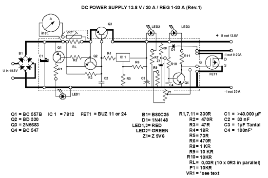
The following DC Power supply circuit is a linear power supply (using transformer). The voltage output of 13.8V power supply is highly regulated, can be adjusted in the moderate range, at up to 20A continuous current. This power supply is suitable for use for amateur radio equipment. DC Power supply is easily constructed and suitable for heavy duty because it is very efficient, small and lightweight.

In the DC power supply presented here, the pass transistors are located in the negative rail and connected in common-emitter configuration rather than as emitter-followers. Thanks to this, the regulator’s minimum voltage drop is extremely low, only about 0.1V for the transistors plus 0.5V for the equalizing resistors.

DC

DC Power Supply Circuit

The other advantage is that the collectors are directly connected to the negative pole of the power supply’s output, which in most applications is grounded. That means that no insulation is required between the transistors and the grounded power supply cabinet! This eases the cooling very considerably. Thanks to the low regulator drop, a low cost 25V filter capacitor can be used.

Some Notes of DC Power Supply Circuit

  • Use a transformer for the primary voltage you need. The 3A fuse is for 220 or 240V primaries. If you use something in the neighborhood of 110V, use a 6A fuse.
  • The rather high transformer rating of 35A accounts for the losses that occur due to the capacitive input filter. If your transformer is rated for capacitive input, then a 25A value is enough.
  • Of course you can make up C1 by placing several smaller capacitors in parallel. Likewise, the 0.1 Ohm, 5 Watt resistors can be made up by several in parallel, for example by 5 resistors of 0.5 Ohm, 1 Watt each.
  • The LM336Z-5.0 voltage reference IC should not be replaced by a zener diode. Zeners are not nearly as stable. A different voltage reference IC can of course be used, if R2 and R3 are modified for the different voltage.
  • D1 and Q2 through Q6 need heatsinking. Only Q2 needs insulation. D1 dissipates up to 60W, Q2 up to 25W, while the pass transistors dissipate up to 30W each in normal use, but may reach a level of 130W during short circuit! Take this into account when choosing the heat sink!
  • R5 exists only to make sure that the transistors can actually be driven off. The 741 is not a single-supply operational amplifier, so it cannot drive its output very low. If a true single-supply opamp is used, then R5 becomes unnecessary.
Read More..

Wednesday, November 12, 2014

STK415 090 E bassed 2x50 watt stereo amplifier Diagram Circuit


This electronic project stereo amp is based on the STK415-090-E class H audio power amplifier hybrid IC that features a built-in power supply switching circuit.
This STK415-090-E class H audio power amplifier provides high efficiency audio power amplification by controlling (switching) the supply voltage supplied to the power devices according to the detected level of the input audio signal.
STK415-090-E class H audio power amplifier is pin to pin compatible with STK416-100 stereo amp .
This electronic project stereo amp will provide an 50 + 50 watts output power with 0.8 % THD , but it can provide more power , up to 80 watts with 10% THD .
STK415-090-E class H audio power amplifier supports output loads from 4 up to 8 ohms and require an input DC voltage from 27 up to 60 volts .
For 8 ohms load , voltage required by this stereo amp project are : +/- 27V for VL and +/-37V for VH .

This 2x50 watt stereo amp project must be designed so that (|VH|-|VL|) is always less than 40V when switching the power supply with the load connected. Set up the VL power supply with an offset voltage at power supply switching (VL-VO) of about 8V as an initial target.
To prevent over heating damage thermal design must be implemented and a thermoplastic adhesive resin must be used for this hybrid IC .
A value of 2.34.C/W, satisfies all required thermal resistance of the heat sink .
Electronic parts required for this 2x50 watt stereo amp electronic project are : R01, R02 1.5k ; R03, R04 100 /1W , R05, R06 56k ; R08, R09 4.7 /1W ; R11, R12 4.7, R14,R15 560 ; R18, R19 56k ; R21, R22 1k ; R24, R26 0.22 10%, 5W ; C01, C02 100.F/100V ; C03, C04 100.F/50V ; C05, C06 100.F/ 100V ; C07, C08 3pF; C10, C11 0.1.F; C13, C14 22.F/10V ; C16, C17 2.2.F/50V ; C19, C20 470pF ; C22, C23 100pF ; D01, D02 15V ; D03, D04 3A/60V ; L01, L02 3.H .

Read More..

Thursday, October 30, 2014

0 3 to 1 5V LED Flashlight Circuit Diagram


Its a little wisp of a circuit that allows you to drive a blue or white LED from a low voltage. Normally, if you want to light up a blue or white LED you need to provide it with 3 - 3.5 V, like from a 3 V lithium coin cell. But a 1.5 V battery like a AA cell simply will not work. But using the Joule Thief, it works like a charm. Not only does it work with a brand new battery, but it works until the battery is nearly dead-- down to 0.3 V. Thats well below the point where your other toys will tell you the battery is dead, so it can steal every last joule of energy from the battery (hence the name). To learn how to make one, watch the video, which is available in a variety of formats.

0.3 to 1.5V LED Flashlight Circuit Diagram


Read More..

Tuesday, October 28, 2014

LM3909 bassed Continuity tester circuit diagram

A very simple continuity tester electronic project can be designed using the LM3909 LED flasher integrated circuit .

This continuity tester project , require few external electronic parts and can be used for testing continuity of coils and cables .
This continuity tester project must be powered from a 1.5 volt DC power supply , you can use a 1.5 volts battery cell .

The C1 capacitor must have a value of 10uF an R1 resistor must a have a value of 1kohms . Speaker used for this project can be a small 8 ohms impedance speaker .
Simple
Read More..

Circuit 3 LED battery monitor

This is the circuit diagram of a 3 LED bar graph type battery monitor circuit that is ideal for monitoring the voltage level of an automobile battery.When battery voltage is 11.5V or less transistor Q1 will be On and the LED D1 will be glowing.When battery voltage is between 11.5 and 13.5V, the transistor Q2 will be On and the LED D2 will be glowing.When battery voltage is above 13.5V the transistor Q3 will be On and the LED D7 will be glowing.

Circuit diagram with Parts list.

Notes.
Assemble the circuit on a general purpose PCB.The battery to be monitored can be connected between the terminals namely A and B.It is always better to use LEDs of different colour.

Read More..

Sunday, October 26, 2014

High End Power Amplifier Circuit

Given is a pretty generic High-End Power Amplifier. Circuit Schematic quite similar to the one that ghosts around the block as "The G0ldm0uth" Amplifier over at DIYA, but with bipolar tripple emitter follower output and not mosfets, output runs at a fair bit of bias current, around 1 Amp in total and uses three complementary pairs of 30MHz (nominal) output transistors.


High-End
High-End Power Amplifier Circuit

Read More..

Intelligent Presence Simulator Diagram Circuit

However effective a domestic alarm system may be, it’s invariably better if it never goes off, and the best way to ensure this is to make potential burglars think the premises are occupied. Indeed, unless you own old masters or objects of great value likely to attract ‘professional’ burglars, it has to be acknowledged that the majority of burglaries are committed by ‘petty’ thieves who are going to be looking more than anything else for simplicity and will prefer to break into homes whose occupants are away.

Rather than simply not going on holiday – which is also one solution to the problem (!) – we’re going to suggest building this intelligent presence simulator which ought to put potential burglars off, even if your home is subjected to close scrutiny. Like all its counterparts, the proposed circuit turns one or more lights on and off when the ambient light falls, but while many devices are content to generate fixed timings, this one works using randomly variable durations.

Circuit diagram:

Intelligent Presence Simulator Circuit Diagram

So while other devices are very soon caught out simply by daily observation (often from a car) because of their too-perfect regularity, this one is much more credible due to the fact that its operating times are irregular. The circuit is very simple, as we have employed a microcontroller – a ‘little’ 12C508 from Microchip, which is more than adequate for such an application. It is mains powered and uses rudimentary voltage regulation by a zener diode.

A relay is used to control the light(s); though this is less elegant than a triac solution, it does avoid any interference from the mains reaching the microcontroller, for example, during thunderstorms. We mustn’t forget this project needs to work very reliably during our absence, whatever happens. The ambient light level is measured by a conventional LDR (light dependent resistor), and the lighting switching threshold is adjustable via P1 to suit the characteristics and positioning of the LDR.

Note that input GP4 of the PIC12C508 is not analogue, but its logic switching threshold is very suitable for this kind of use. The LED connected to GP1 indicates the circuit’s operating mode, selected by grounding or not of GP2 or GP3 via override switch S1. So there are three possible states: permanently off, permanently on, and automatic mode, which is the one normally used. Given the software programmed into the 12C508 (‘firmware’) and the need to generate very long delays so as to arrive at lighting times or an hour or more, it has been necessary to make the MCU operate at a vastly reduced clock frequency.

PCB Layout:

PCB Layout Of Intelligent Presence Simulator

In that case, a crystal-controlled clock is no longer suitable, so the R-C network R5/C3 is used instead. For sure, such a clock source is less stable than a crystal, but then in an application like this, that may well be what we’re after as a degree of randomness is a design target instead of a disadvantage. Our suggested PCB shown here takes all the components for this project except of course for S1, S2, and the LDR, which will need to be positioned on the front panel of the case in order to sense the ambient light intensity.

The PCB has been designed for a Finder relay capable of switching 10 A, which ought to prove adequate for lighting your home, unless you live in a replica of the Palace of Versailles. The program to be loaded into the 12C508 is available for free download from the Elektor website as file number 080231-11.zip or from the author’s own website: www.tavernier-c.com. On completion of the solder work the circuit should work immediately and can be checked by switching to manual mode.

The relay should be released in the ‘off’ position and energized in the ‘on’ position. Then all that remains is to adjust the day/night threshold by adjusting potentiometer P1. To do this, you can either use a lot of patience, or else use a voltmeter – digital or analogue, but the latter will need to be electronic so as to be high impedance – connected between GP4 and ground. When the light level below which you want the lighting to be allowed to come on is reached, adjust P1 to read approximately 1.4 V on the voltmeter.

If this value cannot be achieved, owing to the characteristics of your LDR, reduce or increase R8 if necessary to achieve it (LDRs are known to have rather wide production tolerances). Equipped with this inexpensive accessory, your home of course hasn’t become an impregnable fortress, but at least it ought to appear less attractive to burglars than houses that are plunged into darkness for long periods of time, especially in the middle of summer. (www.tavernier-c.com)

COMPONENTS LIST
Resistors
R1 = 1k 500mW
R2 = 4k7
R3 = 560R
R4,R6 = 10k
R5 = 7k5
R 7 = LDR
R8 = 470k to 1 M
P1 = 470k potentiometer
Capacitors
C1 = 470µF 25V
C2 = 10µF 25V
C3 = 1nF5
C4 = 10nF
Semiconductors
D1,D2 = 1N4004
D3 = diode zener 4V7 400 mW
LED1 = LED, red
D4 = 1N4148
T1 = BC547
IC1 = PIC12C508, programmed, see Downloads
Miscellaneous
RE1 = relay, 10A contact
S1 = 1-pole 3-way rotary switch
F1 = fuse 100 mA
TR1 = Mains transformer 2x9 V, 1.2 -3 VA
4 PCB terminal blocks, 5 mm lead pitch
5 solder pins 
Read More..

Saturday, October 25, 2014

OP270E Low Noise Microphone Amplifier Diagram Circuit

The signal from a microphone is two weak for a standard line input. This low-noise DC-coupled microphone amplifier provides a solution for anyone who wants to connect a microphone to his or her hi-fi installation. As can be seen from the schematic diagram, a good circuit does not have to be complex. A differential amplifier is built around T1 (MAT-03E), which is a low-noise dual transistor. The combination of T2 and LED D1 forms a constant-current source for the input stage. A low-noise opamp (OP-270E) amplifies the difference signal that appears at the collectors of the dual transistor. The result is an analogue signal at line level.

Low-NoiseThe bandwidth of the amplifier ranges from 1 Hz to 20 kHz. Within the audio range (20 Hz to 20 kHz), the distortion is less than 0.005 percent. Since only half of the OP-270E is used, the remaining opamp could be used in the output stage of a stereo version. The amplifier can be powered from a stabilized, symmetrical supply with a voltage between ±12 V and ±15 V. Such supply voltages are already present in many amplifier
Read More..

Friday, October 24, 2014

FM Radio Receiver Circuit with IC TDA 7012T

FM Radio Receiver IC TDA 7012T is very simple, but it has an FM radio receiver sensitivity and good selectivity. Single Chip FM Receifer cool name of IC TDA7012T 7012T TDA is to build an FM receiver requires a few additional components. 
Feature contained in FM receiver IC TDA 7012T is quite tempting to an FM receiver. Among features an FM receiver TDA 7012T is a low-voltage applications micro affability arrangement (MTS), Frequency Loked Loop (FLL) to 76 KHz range and selectivity of FM receiver with RC Filter. In an article by FM Radio Receiver IC TDA 7012T can be seen in the FM receiver circuit which can be made​​.


FM Radio Receiver with IC TDA 7012T

From the picture above components to make the FM Radio Receiver IC TDA 7012T as follows:

R1 = 8kΩ2
R2 = 10kΩ
R3 = 390Ω
C1, C3 = 10nF
C2, C6, C9, C16 = 100nF
C4 = 33pF
C5 = 25pF trimmer
C7, C10 = 1nF5
C8 = 820pF C11 = 1NF
C12 = 68pF
C13 = 220pF
C14 = 47μF 10V
C15 = 3nF3
L1 = 36nH
L2 = 1μH,
IC1 = TDA7021T
Read More..

Thursday, October 23, 2014

Running Light circuit uses a CMOS 555 timer

A Transcutaneous Electrical Nerve Stimulation (TENS) device is, put bluntly, a machine for giving electric shocks. The author was prescribed such a device on loan by his orthopaedic specialist. The unit has a large number of programmes, of which he used only one. Measuring the signals at the output of the device in this mode revealed damped oscillations at a frequency of approximately 2.5 kHz, with a repetition rate of approximately 100 Hz.
Running Light circuit uses a CMOS 555 timer

How hard can it be to make such a device ourselves? The simple circuit uses a CMOS 555 timer to produce a brief pulse which feeds a 1:10 miniature transformer. Together with a 4.7 nF capacitor the transformer makes a parallel resonant circuit: the resonance leads to a considerable increase in the output voltage. The pulse width can be adjusted using a potentiometer, here shown combined with the on-off switch. Wider pulses produce higher output voltages. Since a peak voltage of up to 200 V can be produced, the transformer must have adequate insulation: Conrad Electronics type 516260-62 is suitable. A low-cost phono socket at the output gives reliable connection to the electrode cable.

The adhesive electrodes shown in the photograph (disposable and permanent types are available) can be obtained from pharmacies and medical suppliers. They generally have connectors compatible with 2 mm banana plugs, and so it is possible to make up the necessary cable yourself. To treat responsive parts of the body, such as the arm, the potentiometer need not be turned up far to obtain the necessary sensation. Less sensitive parts, such as the knee or foot, need a rather higher voltage and hence a correspondingly higher potentiometer setting.

Author: Klaus Rohwer – Copyright: Elektor Electronics Magazine
Link:http://www.extremecircuits.net/2010/06/transcutaneous-electrical-nerve_03.html
Read More..

Saturday, October 18, 2014

Headlight Reminder circuit and explanation

With the storm season recently upon us, it’s not uncommon to switch car headlights on during the daytime. Unfortunately, it’s easy to forget to turn them off again when parking, with the result being a flat battery. This circuit will sound an alarm if the ignition switch is moved to the "off" position while the car lights are on, reminding you to turn the lights off before leaving the vehicle. The circuit is simple but effective. A 555 timer (IC1) is configured as a free-running oscillator to drive a small piezo transducer. The pitch of the transducer is set by the resistor and capacitor connected to pins 2 & 6. Power for the 555 is derived from the dashboard lighting circuit. However, the piezo does not sound during normal operation, because the 555’s reset input (pin 4) is held low by transistor Q1.

Circuit diagram:
Headlight Reminder Circuit Diagram

This transistor is switched on whenever accessory power is present, pulling its collector towards ground (0V). If the ignition is switched off but the lighting circuit remains powered, the loss of accessory power results in Q1 switching off and releasing the reset signal to IC1, sounding the alarm. A 220Ω resistor in series with the piezo protects the 555’s output (pin 3). Although most piezo elements have relatively high impedance, this drops as the frequency increases due to their capacitive nature. The square-wave output on pin 3 includes many harmonics, some extending well into the ultrasonic range. The unit fits easily into a small plastic box. I spliced mine into the wiring running to the cigarette lighter, which includes both accessories and panel lamp circuits as well as a chassis ground wire. The result fits neatly behind the ashtray, with no chassis bashing required!

Author: Bruce Colledge - Copyright: Silicon Chip Electronics
Read More..