Showing posts with label audio. Show all posts

Sunday, November 16, 2014

Car audio amplifier using TDA2003 IC


Easy low power car audio amplifier circuit on TDA 2003. The circuit is Easy to construct. TDA2003 is an integrated radio amplifier from ST Micro electronics that like short circuit protection for all pins, thermal over low harmonic distortion, low cross over distortion etc. In the circuit given here TDA2003 is wired as a mono amplifier operating from a 12V .

Resistors R2 and R3 forms a feedback network that sets the amplifiers gain. C7 input DC de-coupling capacitor and C5 couples the speaker to the amplifiers output. C4 } for improving the ripple rejection C1 and C2 are employed for power filtering. C3 and R1 are used for setting the frequency cut-off. Network comprising of C6 and R4 for frequency stabilization and oscillation.

Notes.

  • Assemble the circuit on a good quality PCB.
  • Heat sinks are necessary for both ICs.
  • The circuit can be operated from 12V DC.
  • S1 is the ON/OFF switch.
Read More..

Sunday, November 2, 2014

AUDIO LEVEL METER ELECTRONIC DIAGRAM


AUDIO LEVEL METER ELECTRONIC DIAGRAM

It consists of only few components. IC LM3915 converts the audio analog voltage and display it to the LED. Here is the schematic :

Parts list :
  •     Resistor R1 : 1k2
  •     Resistor variable R2 : 10k
  •     IC : LM3915
  •     LED indicator LED1-LED10 : LED 5mm
  •     12V power supply
Read More..

Wednesday, October 29, 2014

Collection Scheme Audio Power Amplifier High Power MOSFETs

200W Audio Amplifier with Mosfet BUZ905P-BUZ900P

This project is develop from the MOSFET Power amplifier 100W that posted which it take to use in many activity such as Guitar amp,Mic,or Home theater and you will be to apply it.
As many people prefer because of its robustness MOSFET legendary. Altronics had a MOSFET amplifier with 200W, the product in a 4Ω, and we have decided to take a look at is.
It turns out that on the basis of the Pro One “, as described above, even if this version of Altronics and to the various MOSFETs. He has a rated output of 140W to 200W into 4Ω and 8W. Frequency range of 1 dB 20Hz up to 80kHz (Fig. 1). THD is less than 0.1% at full power (Fig. 2) and signal to noise ratio when compared to 200W is better than -100 dB unweighted.
Performance of the prototype
Output power (RMS ):… 140W into 8 ohms, 200W into 4 ohms
Frequency Response:. 20Hz – 80kHz-1dB points (see Figure 1)
Input sensitivity: ………… 830mV for 200W into 4 ohms
Distortion: … <0.1% (20 Hz – 20 kHz) (see Fig.2)
Signal-to-Noise Ratio:. > 102dB unweighted, 105dB A-weighted with respect to 200W into 4 ohms
Stability :…………………….. Unconditional
Originally, the “Pro Series One” was developed by Hitachi MOSFET A-3 metal containers. They are no longer available, and their counterparts from plastics are very difficult to obtain. Altronics on this situation and have essentially the same circuits designed for Plastic MOSFET corresponds Exicon by the United Kingdom. This required a re-design of the computer, so that all MOSFET and the pilot for all transistors on a plate are vertically mounted on the radiator.
Besides the use of plastic in the power transistors, which greatly simplifies the assembly of the metal in comparison with A-3 power transistors, have Altronics spring clips in the proximity of the pairs of transistors, so things were still simple. The spring clips, just what the voltage for transistors and there is no harm in a transistor due to struggle more screws.
The heat sink is a black anodized aluminum extrusion with fins on one side. It measures 300 mm long and has a lid that a 80mm fan cooled 24V DC. The fan runs constantly, which means that the radiator is always cool (or at least slightly above the ambient temperature).

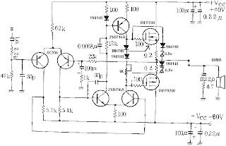
100W Audio Amplifer Circuit With MOSFET IRFP240

MOSFET amplifier with MOSFET for your build in electronic hobby.
I would like to show you here a basic MOSFET amplifier or power Amp which Output power is plus/minus 100 Watt/RMS with
8 Ohms or ohter plus/minus 160 Watts /RMS with 4 ohms.
Regarding this circuit simplicity, The distortion is plus/minus 0.1 %.
For band-width -3 db(decibel) is gain for 4 Hz to 96 Khz, it is limited by C1, R1, C2 and R2.
In the two transistors are T1 and T2 makes a first differential stage part, So,current source(I) of +/- one mA is set with resistor R3.

For the upgraded project, The current source(I) is more efficient in stability. Coil P1 allows a fine tuning of direct current voltage at amplifier’s output. Place the Coil P1 with it’s half value for first power up, then turn it slowly for a lowest DC output voltage. Use a first quality compoment.
Electronic Part
C1 = 2,2 µF MKP, MKT 100 V
C2 = 330 pF céramique 50 V
C3 = 100 nF MKP, MKT 100 V
C4 = 100 µF 40 V électro-chimique
C5, C6 = 18 pF céramique 50 V
C7 = 100 nF MKP, MKT 250 V  (C8 = 47 µF 100 V)
R1, R3 = 47 K   (R3 = 330 -> 470 Ohms)
R2 = 2K2
R4, R5 = 3K9
R6 = 1 K
R7 = 27 K
R8, R9, R11 = 100 ohms
R10 = 10 K
R12, R13 = 470 ohms
R14, R15 = 0.33 ohms 5 watts
R16 = 10 ohms 3 watts      (R17 = 1 K    R18, R19 = 10K)
T1, T2, T9,T10 = 2SD756A,2SD716A, BC556B (attention au brochage différent – take care for pin layout)
T7 = IRFP240, 2SK1530, 2SJ162, BUZ900DP, BUZ901DP (attention au brochage different – take care for pin layout : GDS GSD)P1 = 100 ohms  (25 tours – 25 turns)

230W Audio Amplifer Circuit With MOSFET IRFP240,9240

230 W MOSFET Audio Amplifer Circuit Here is simple LED-power audio amplifier circuit with MOSFET amplifier TL071C and 2 may be up to 45 W into 8 ohms.

For MOSFET IRFP240 and IRFP9240 are used safety with device can now be these modification.
The scheme is at the request SILICONIX and the voltage change of 2 serial resistances from suppliers operating voltage amplifier driver was inserted.
MOSFET must be mounted on at least one condenser 1K / W.
Amplifier efficiency is 70%, the reduction in the frequency distortion in more than 0.2% at 20 Hz at 8 ohms and 10W.
With a supply voltage in the range of + – 30V, can supply audio amplifier MOSFET 45W into 8 ohms and 70W into 4 ohms.
Remember that the sound amplifier is short, so all you can check the radio button is protected, whether the speaker is connected.


400Watt Audio Power Amplifier with Mosfet BUZ902DP

If you like in the sound system or sound this circuit will should like you , This amplifier has two completely separate mono amplifiers with each channel has its own power supply to the order of zero channel crosstalk, a common phenomenon in amplifiers have the same food.
To view the full performance of each supply transformer should be evaluated at 40VAC – 0 – 40VAC at 640VA.
Unlike many models of capacitors is a reservoir to supply the peak currents, I prefer the power transformer in a much faster transient. BUZ902DP Although the specifications are rather modest,
if they can hear you now to experience a large reserve of power available and never any reason to worry that something to do than drive a large number of amplifiers aloud. You do not hear nothing but the truth without distortion at all levels, and I can assure you that this amplifier is required to provide the best features coupled.

800 Watt Audio Amplifer circuit with MOSFET

800W audio amplifier circuit
The audio power amplifier ideal for home user or PA work or for use as a general-purpose subwoofer or hi-fi amplifier. There are many people like to prefer MOSFET as their legendary ruggedness.
This circuit project had the Mosfet amplifier module which produced 800 Watt  into 4 Ohm speaker load and so we decided to take a look it.
It was turned out to be based on the “Pro Series One” as mentioned above, although this version by Altronics has had derated and adapted to different MOSFET. It has a  power output rate with 700W into 8W and 800W into 4 Ohm. For frequency response is within 1dB from 20Hz to 80kHz. Total harmonic distortion is rated at less than 0.1% up to full power and signal-to-noise ratio with respect to 800W is better than 100dB unweighted.
For circuit using MOSFET number BUZ902DP ,BUZ907DP which is popula take to build amplifer, If you see the circuit ,It seen 2 same circuits in the project which one circuit can gen power output at 400 Watt.


1000W MOSFET Audio Amplifier Circuit

Welcome to Hobby Electronics ,Today i’m still present the audio amplifier circuit ,I like the supper amplifier .
So,I would like to show you the 1000Watts  MOSFET amplifier circuit for your build sound system.
Click the picture left side to open the Circuit in PDF file.
I include full schemaatic chart and film; pattern of the 1000-watt amplifier and a step by step instructions for setting the construction of the amplifier is a true full 1000 watts per channel.
 I have been building and playing very well goood can drive a 18 Bring with inch subwoofer dual magnet high performance at UA smooth clear and crisp sound that I used for outdoor event and mobile services when building you will, said this amp I can only contact me gave my email Mail on how to get this project … I assure you his powerful …. You could, but I have to return it a full program of 20 band equalizer can be difficult to find on the net …
Read More..

Automatic Switch For Audio Power Amplifier

Circuit of an automatic switch for audio power amplifier stage is presented here. The circuit uses stereo preamplifier output to detect the presence of audio to switch the audio power amplifier on only when audio is present. The circuit thus helps curtail power wastage. IC1 is used as an inverting adder. The input signals from left and right channels are combined to form a common signal for IC2, which is used as an open loop comparator. IC3 (NE556) is a dual timer. Its second section, i.e., IC3(b), is configured as monostable multivibrator. Output of IC3(b) is used to switch the power amplifier on or off through a Darlington pair formed by transistors T1 and T2. IC3(a) is used to trigger the monostable multivibrator whenever an input signal is sensed.

Circuit diagram:
Automatic
Automatic Switch For Audio Power Amplifier Circuit Diagram

Under ‘no signal’ condition, pin 3 of IC2 is negative with respect to its pin 2. Hence the output of IC2 is low and as a result output of IC3(a) is high. Since there is no trigger at pin 8 of IC3(b), the output of IC3(b) will be low and the amplifier will be off. When an input singal is applied to IC1, IC2 converts the inverted sum of the input signals into a rectangular waveform by comparing it with a constant voltage which can be controlled by varying potentiometer VR1. When the output of IC2 is high, output pin 5 of IC3 goes low, thus triggering the monostable multivibrator. As soon as the audio input to IC1 stops, pin 5 of IC3 goes high and pin 1 of IC3 discharges through capacitor C3, thus resetting the monostable multivibrator. 

Hence, as long as input signals are applied, the amplifier remains ‘on.’ When the input signals are removed, i.e., when signal level is zero, the amplifier switches off after the mono flip-flop delay period determined by the values of resistor R8 and capacitor C3. If no input signals are sensed within this time, the amplifier turns off—else it remains on. Power supply for the circuit can be obtained from the power supply of the amplifier. Hence, the circuit can be permanently fitted in the amplifier box itself. The main switch of the amplifier should be always kept on. Resistors R1 and R2 are used to divide single voltage supply into two equal parts.

Capacitors C1 and C2 are used as regulators and also as an AC bypass for input signals. Diode D1 is used so that loading fluctuations in power amplifier do not affect circuit regulation. Transisitor T2 acts as a high voltage switch which may be replaced by any other high voltage switching transistor satisfying amplifier current requirements. Value of resistor R10 should be modified for large current requirement. The LED glows when the amplifier is on. The circuit is very useful and relieves one from putting the amplifier on and off every time one plays a cassette or radio etc. 


Source : EFY
Read More..

Thursday, October 16, 2014

TV audio video transmitter Schematic Diagram

This is a simple TV audio video transmitter circuit can be constructed using this schematic diagram . This TV audio video transmitter circuit can be used to transmit video signals from VCR ( or some other device ) to a TV without using any cable .

Video signals input at jack J1 are first terminated by resistor R6 and coupled through capacitor C1 to clamping-diode D1. Potentiometer R3 is used to set the gain of the video signal; its effect is similar to that of the contrast control on a TV set.

TV audio video transmitter Schematic Diagram

TV
 

Bias-control R7 can be used to adjust the black level of the picture so that some level of signal is transmitted, even for a totally dark picture.

RF-transformer T1 and its internal capacitor form the tank circuit of a Hartley oscillator thats tuned to 4.5 megahertz. Audio signals input at J2 are coupled to the base of Q3 via C2 and R4: the audio signal modulates the base signal of Q3 to form an audio subcarrier that‚s 4.5-megahertz higher than the video-carrier frequency.

The FM modulated subcarrier is applied to the modulator section through C5 and R9.
Resistor R9 adjusts the level of the subcarrier with respect to the video signal.

Transistors Q1 and Q2 amplitude modulate the video and audio signals onto an RF-carrier signal. The operating frequency is set by coil L4, which is 3.5 turns of 24- gauge enameled wire on a form containing a standard ferrite slug.

The RF output from the oscillator (L4, C7 and C9 ) section is amplified by Q5 and Q6, whose supply voltage comes from the modulator . Antenna matching and low-pass filtering is performed by C12, C13, and L1.

Resistor R12 is optional; it is added to help match the output signal to any kind of antenna.
To align this audio video transmitter you need to tune a TV receiver to an unused channel between 2 and 6. The TV must have an indoor antenna connected directly to it; an outdoor antenna or cable wont work. Make sure both potentiometers (R3, R7) are in middle position and apply power to the transmitter. Adjust L4 with a nonmetallic tool until the TV screen goes blank ,then fine-adjust L4 for the "most-blank" picture.
Connect the video and audio outputs from a VCR(AV source) to jacks J1 and J2 (respectively) of the transmitter .

After that you should see a picture on the TV screen: if you do, readjust L4 for the best picture; if you dont, check the board for any bad connections. Next, adjust R3 for the best picture brightness and R7 for the best overall picture.

Finally, adjust T1 with a nonmetallic tool for the best sound .
The TV transmitter combines line level audio and video signals, and transmits the resulting signal up to 300 feet. The circuit can be powered from a 9-12V power supply circuit .

Read More..

Thursday, September 18, 2014

10W AUDIO AMPLIFIER WITH MUTING

DESCRIPTION

The TDA 1910 is a monolithic integrated circuit in MULTIWATT® package, intended for use in Hi-Fi audio power applications, as high quality TV sets. The TDA 1910 meets the DIN 45500 (d = 0.5%) guaranteed output power of 10W when used at 24V/4W. At 24V/8W the output power is 7W min.


Features:

  • muting facility
  • protection against chip over temperature
  • very low noise
  • high supply voltage rejection
  • low "switch-on" noise.
  • easy assembly
  • simple heatsink
Circuit Diagram
10W AUDIO AMPLIFIER WITH MUTING

Read More..

Monday, September 15, 2014

50W audio amplifier LM3876 Wiring diagram Schematic

LM3876 is a high performance audio power amplifier IC from National Semiconductors. The LM3876 can deliver 50watts of output power into an 8 ohm loudspeaker. LM3876 has excellent signal to noise ratio and has wide supply voltage range. Other features of LM3876 are output to ground short schema protection, input mute function, and output over voltage protection, etc. Applications of LM3876 are component stereo, compact stereo, surround systems, self powered speakers, etc.

Circuit diagram :

50W audio amplifier Circuit Diagram

The 50 watt audio amplifier  schema shown below is designed based on the application diagram from the data sheet of LM3876. Some modifications are made on the original schema for improving the performance. The bipolar electrolytic capacitor C7 is the input DC decoupling capacitor. R4 is the input resistance. R2 & R1 and bipolar electrolytic capacitor C5 forms a feedback schema. C2, C1 are filter/by-pass capacitors for the positive supply rail. C4 & C3 are the filters/by-pass capacitors for the negative supply rail. The feedback resistor R2 sets the gain of the amplifier. L1 provides high impedance at high frequencies so that R7 may decouple capacitive loads. R3 is the mute resistance which allows 0.5mA to be drawn from pin8 to turn the mute function OFF. S1 is the mute switch. Resistor R6 and capacitor C8 forms a Zobel network which improves the high frequency stability of the amplifier and prevents oscillations.

Notes :
  • The LM3876 can be operated from a supply voltage range of +/-12V to +/-49V DC.
  • I recommend +/-35V DC for powering the IC.
  • LM3876 requires a proper heat sink.
  • Quiescent current of LM3876 is around 70mA
Read More..

Saturday, September 13, 2014

NPD8301 FET Audio Amplifier

The excellent characteristics for the track NPD8301 over its range of bias current, thereby improving common mode rejection. The monolithic double NPD8301 offers an ideal low offset buffer function LM10lA low drift op amp.

Read More..

Friday, September 12, 2014

Audio power amplifier circuit based on TDA4920 TDA4925 TDA4930

Specification :
This is stereo amplifier , based on IC TDA4920 , TDA4925 , TDA4930 . Minimum voltage require 9 volts and maximum voltage 13 volts . Maximum power output 2 x 15 Watts with 4 Ohms impedance. Quiescent current 30 mA. See audio circuit scheematic below :


Read More..

Sunday, September 7, 2014

6 5W audio power amplifier

This amplifier circuit based on the ic, and the use here is that where ic STK4017 IC has output power of 6.5 watts with the impedance 8Ohm. Minimum required supply voltage and maximum 20Volt 35 Volt DC.
Component
R1 = 100K
R2 = 2K7
R3 = 27R
C1 = 22uF
C2 = 100uF
C3 = 100uF
C4 = 100uF
C5 = 100uF
C6 = 47uF
C7 = 330uF
C8 = 100uF
U1 = STK4017
Besides using STK4017 ic, ic and can use that I mentioned the following:
STK4019
STK4021
STK4023
STK4025
Read More..

Sunday, August 31, 2014

100w audio amplifier

General description:


All resistors are standard metal film 250mW except: R1/3/4/7, these are 2W metal film, and the 0.22ohm beeing 5W. Around R7 is wounded a 0.6mm isolated (enamelled) copper wire forming the output coil. (~12 windings)  For c19 i used 470uf/16v, all other electrolytics 63v. The 10/100/330pF should be mica-caps. The 100nf and 47nf is recommended to be Wima MKS2 (or better), also for C1 i suggest Wima MKS2, 4.7uf is enough. For Trimpot i use a Piher. The MPSA18 can be substituted by BC550C, for all other parts i do not recommend changes, especially the feedback network (r29/30) should be kept unchanged, feedback compensation is very delicate for this circuit ! Be careful when substituting the MPSA18 with BC550C, the pinout is reversed between these 2 transistors !!! The bias is adjusted via the trimpot (R22). Recommended bias is 55ma, resulting in 12mv across a single 0.22ohms or 24mv across both 0.22ohms. Connect a DMM to the upper wires of these resistors and adjust trimpot until DMM reads wanted voltage.

Features:


THD: ~0.005% (measured) simd: 0.002%
Power into 8ohm: 60 watts
Power into 4ohm: 100 watts
Gain: 32dB (~1:40) full output at 0.7v input (0.5v rms)
Feedback: 57dB
GainBandWidth: ~400Mhz
Slewrate: ~20v/us (symetrical)
Supply voltage: +/- 36v
Biasing: 55ma, ~12mv across a single 0.22 ohm
Measurings:The measuring setup itself is far from perfect, but gives a good idea !
Frequency response: 3.2hz to 145khz (-1db) using 4.7uf input cap
Phaseshift at 10khz: <3°
More will follow !

Circuit Diagram:

100w audio amplifier  circuit diagram

Layout Diagram:

100w audio amplifier  layout diagram


Partlist:


Device
Qty
Value
Notes
Q1,Q2
2
MPSA18
can be substituted by BC550C (pins reversed !)
Q7,Q8
2
BC546B
or maybe 2n5551 (pins reversed !)
Q3,Q9
2
2N5551
OnSemi/Fairchild/Philips
Q4,Q5,Q12
3
2N5401
OnSemi/Fairchild/Philips
T1
1
BD139
or bd135, bd135-16
U$5
1
MJE15030
OnSemi
U$6
1
MJE15031
OnSemi
U$3
1
MJL3281A
OnSemi
U$4
1
MJL1302A
OnSemi


Device
Qty
Value
Notes
C14
1
10pF (has been 22pF)
Mica
C2,C7
2
100pF
Mica
C3,C4
2
330pF
Mica
C18
1
47nF
Wima MKS2
C5, C6, C10, C11, C16, C17, C20
7
100nF
Wima MKS2
C1
1
10uF (4.7uF also fits)
Wima MKS2
C8,C9
2
100uF
Electrolytic 63v (at least 40v)
C19
1
470uF
Electrolytic 16v
C12,C13
2
1000uF
Electrolytic 63v (at least 40v)


Device
Qty
Value
Notes
R27,R28
2
0R22
5Watts
R1, R3
2
1R2
2Watts metal film
R4
1
4R7
2Watts metal film
R7
1
10
2Watts metal film
R2
1
10
250mW metal film
R8, R9
2
22
250mW metal film
R31, R32
2
47 (have been 22)
250mW metal film
R26
1
33
250mW metal film
R10
1
68
250mW metal film
R15,R17
2
150
250mW metal film
R11
1
220
250mW metal film
R24,R30
2
499 (or 500)
250mW metal film
R5,R6
2
680
250mW metal film
R13,R23
2
2k
250mW metal film
R12,R14,R29
3
22k
250mW metal film
R18,R20
2
47k
250mW metal film
R22
1
1k pot
Piher, small (470ohm might be better)

Device
Qty
Value
Notes
F1,F2
2
2.5T Fuse
Slow blow
F1,F2
2
---
Fuse holder
L1
1
---
0.6mm isolated (enamelled) copper wire wounded around R7 forming the output coil.

Read More..